Touch panels

a technology of touch panel and driving wire, which is applied in the field of touch technology, can solve the problems of a large amount of tx driving wire, and achieve the effect of reducing the number of driving wires

Active Publication Date: 2018-04-26
SHENZHEN CHINA STAR OPTOELECTRONICS TECH CO LTD
View PDF10 Cites 2 Cited by
  • Summary
  • Abstract
  • Description
  • Claims
  • Application Information

AI Technical Summary

Benefits of technology

[0025]In view of the above, each of the touch electrodes connects to one wiring. The first strobe circuit includes a first end for providing the touch driving signals and at least two second ends, wherein each of the second ends connects to one wiring such that the first end providing the touch driving signals may selectively connect to one of the second ends so as to output the touch driving signals to the wiring connected with the touch electrode via one second end. In this way, the touch driving signals may be respectively provided to the touch electrode so as to realize the touch function of the touch panel. A number of the first ends is smaller than the number of the second ends. That is, the number of the first ends providing the touch driving signals is smaller than the number of the touch electrodes. Thus, the number of the wirings for inputting the touch driving signals to the touch electrodes is smaller than the number of the touch electrodes. Compared to the conventional method, the number of the driving wirings may be reduced, and so does the dimension occupied by the driving wirings, which is beneficial to the narrow border design.

Problems solved by technology

Single-touch solution is only capable of identifying one touch point, that is, single-touch solution cannot identify two points touched at the same time.
As the Tx driving wirings are arranged around the border, a great amount of the Tx driving wirings may against the narrow border design.

Method used


Image

  • Touch panels
  • Touch panels
  • Touch panels

Examples


Embodiment Construction

[0039]Embodiments of the invention will now be described more fully hereinafter with reference to the accompanying drawings, in which embodiments of the invention are shown.

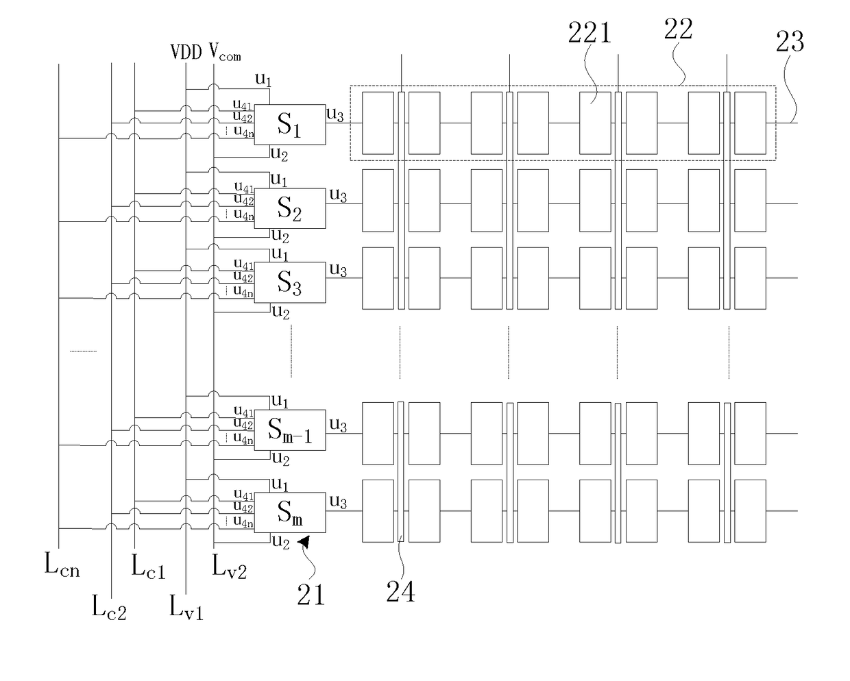
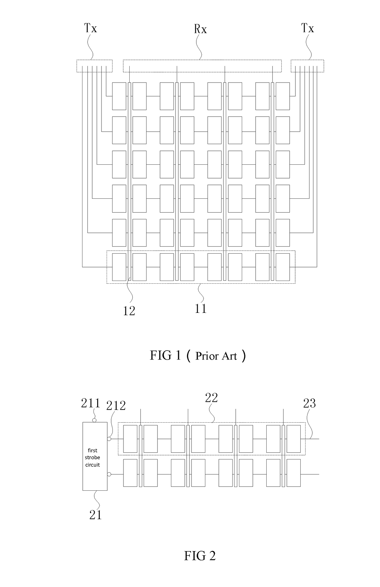
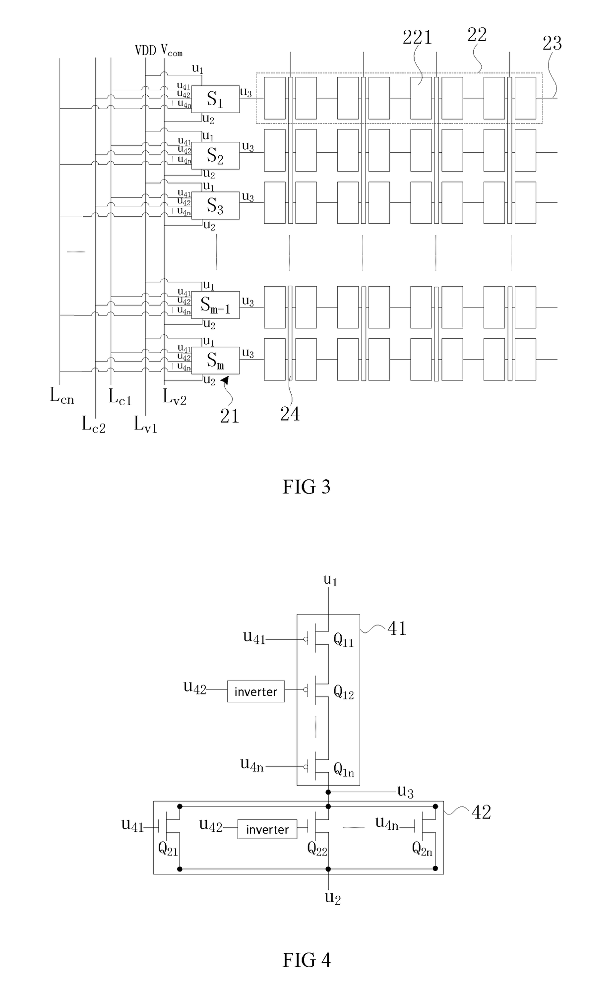
[0040]Referring to FIG. 2, in one embodiment, the touch panel includes a first strobe circuit 21, at least two touch electrodes 22 arranged along a row direction, and at least two wirings 23 respectively connecting with each of the touch electrodes 22.

[0041]The first strobe circuit 21 includes at least two first ends 211 and at least two second ends 212. The first end 211 is configured for providing the touch driving signals. The number of the first ends 211 is smaller than the number of the second ends 212. Each of the second ends 212 directly connects with one wiring 23 so as to connect with one touch electrode 22. The first end 211 selectively connects to one of the second ends 212 such that the first strobe circuit 21 providing the touch driving signals selectively connects to one of the touch electrodes 22. ...


PUM

PropertyMeasurementUnit
voltageaaaaaaaaaa
capacitanceaaaaaaaaaa
mutual capacitanceaaaaaaaaaa

Abstract

A touch panel includes a first strobe circuit, at least two touch electrodes arranged along a row direction, and at least two wirings connecting with each of the touch electrodes. The first strobe circuit includes at least two first ends and at least two second ends, one of the first end is configured for providing touch driving signals, each of the second ends directly or indirectly connects with one wiring, a number of the first ends is smaller than the number of the second ends, and the first end for providing the touch driving signals selectively connects to one of the second ends. In this way, the number of the driving wirings may be reduced, and so does the dimension occupied by the driving wirings, which is beneficial to the narrow border design.

Description

BACKGROUND OF THE INVENTION1. Field of the Invention[0001]The present disclosure relates to touch technology, and more particularly to a touch panel.2. Discussion of the Related Art[0002]Liquid crystal device (LCD) is the most widely adopted display device, and have been incorporated in the display having high resolution, such as mobile phones, PDAs, digital cameras, displays for computers and notebooks. In addition, with the development of liquid crystal display, user demands toward display performance, outlook design and human-machine interfaces have been proposed. Touch technology has been a main trend due to attributes, such as easy to use, endurable, and easy to communicate.[0003]Touch technology mainly includes single-touch and multi-touch solutions. Single-touch solution is only capable of identifying one touch point, that is, single-touch solution cannot identify two points touched at the same time. Multi-touch solution mainly includes two tasks. One of the tasks relate to c...

Claims


Application Information

Patent Timeline
Patent Type & Authority Applications(United States)
IPC IPC(8): G06F3/047G02F1/1333G02F1/1343
CPCG06F3/047G02F1/13338G02F1/134309G06F2203/04103G06F3/0412G06F3/044G06F2203/04111G09G3/3674G06F3/04164G06F3/04166G06F3/0446
Inventor HAO, SIKUN
Owner SHENZHEN CHINA STAR OPTOELECTRONICS TECH CO LTD
Why Eureka
Try Eureka