
Array substrate and touch display device

Inactive Publication Date: 2018-04-26
WUHAN CHINA STAR OPTOELECTRONICS TECH CO LTD
View PDF1 Cites 5 Cited by
  • Summary
  • Abstract
  • Description
  • Claims
  • Application Information

AI Technical Summary

Benefits of technology

The present invention provides a solution to the light leakage problem in touch display devices by introducing a shield line between the common electrodes. This shield line has the same electrical potential as the common electrode and shields the electrical field generated by the data line, thus avoiding effects on the rotations of liquid crystals. The technical effect of this invention is the improvement of the display quality of touch display devices.

Problems solved by technology

However, the existing technologies have at least the following technical problems.
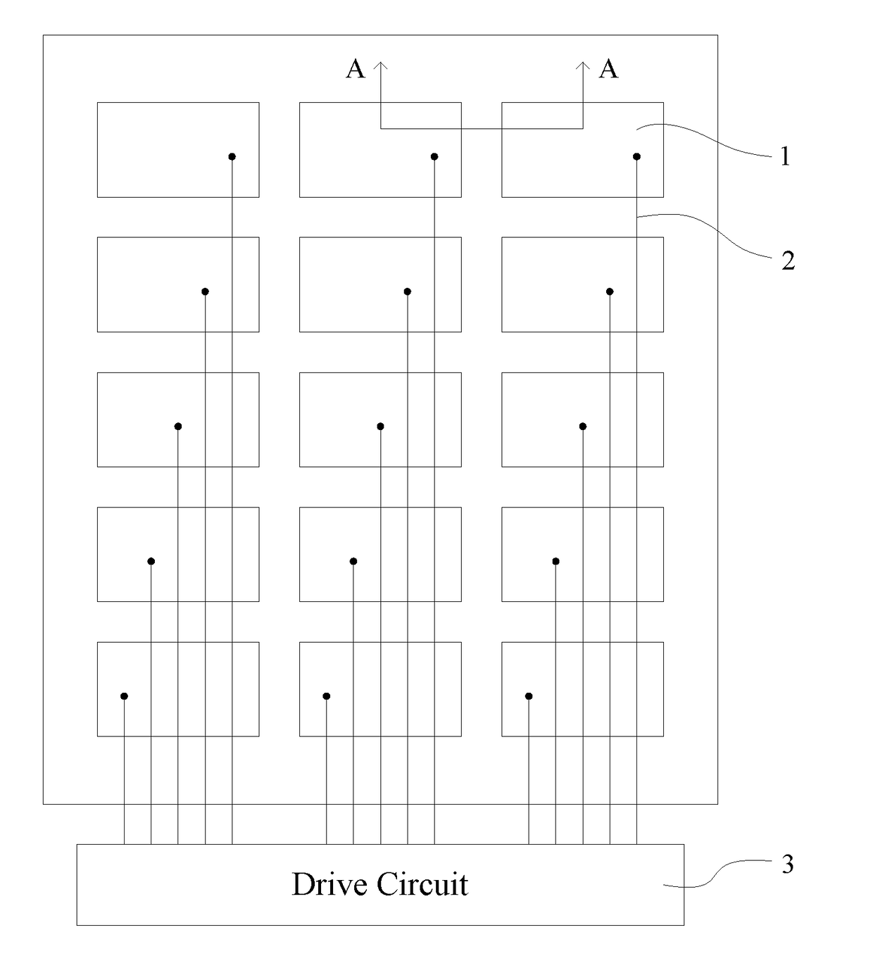
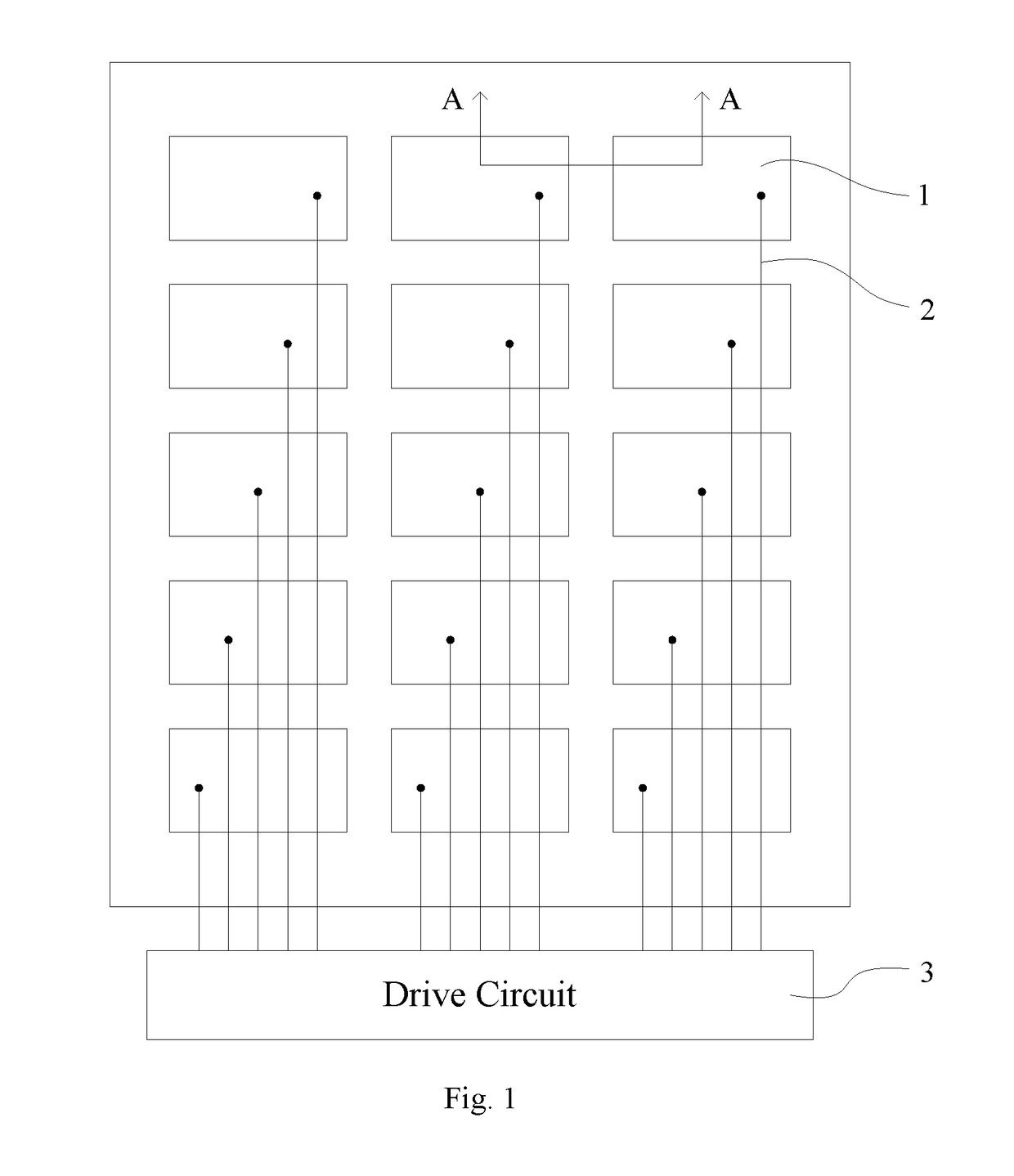
But when a data line 4 transmits signal, an electrical field generated by the data line will go through a gap between the common electrodes 1 and consequently interfere with rotating directions of liquid crystals 5 near the gap, thereby leading to light leakage near the gap.

Method used


Image

  • Array substrate and touch display device
  • Array substrate and touch display device
  • Array substrate and touch display device

Examples


embodiment 1

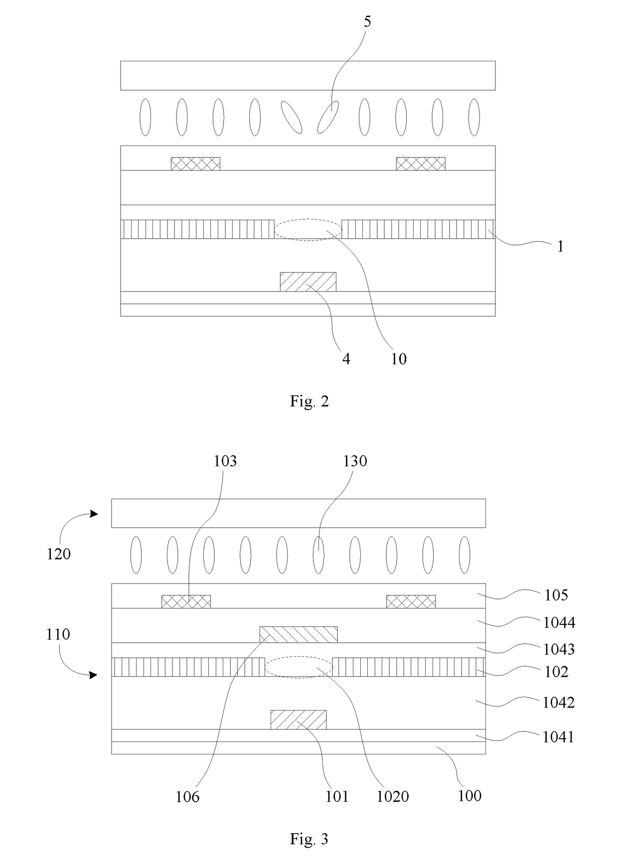
[0025]The present embodiment provides a touch display device, which can be used as the touch display device for electrical products, such as mobile phones and tablet PCs, which adopt in-cell technology. As shown in FIG. 3, the touch display device comprises an array substrate 110, a color filter substrate 120, liquid crystals 130, a drive circuit (not shown in the Fig.), etc.

[0026]The array substrate 110 comprises, from bottom to top, a base substrate 100, a first metal layer, a first insulating layer 1041, a second metal layer, a second insulating layer 1042, a first transparent electrode layer, a third insulating layer 1043, a third metal layer, a fourth insulating layer 1044, a second transparent electrode layer, an alignment layer 105, etc., in turn. The array substrate specifically comprises a sub-pixel unit array formed by a plurality of gate lines (not shown in the Fig.) and a plurality of data lines 101, and also a plurality of common electrodes 102. The gate lines are locat...

embodiment 2

[0034]The present embodiment provides a touch display device, which can be used as the touch display device for electrical products, such as mobile phones and tablet PCs, which adopt in-cell technology. As shown in FIG. 4, the touch display device comprises an array substrate 210, a color filter substrate 220, liquid crystals 230, a drive circuit (not shown in the Fig.), etc.

[0035]The array substrate 210 comprises, from bottom to top, a base substrate 200, a first metal layer, a first insulating layer 2041, a second metal layer, a second insulating layer 2042, a first transparent electrode layer, a third insulating layer 2043, a third metal layer, a fourth insulating layer 2044, a second transparent electrode layer, an alignment layer 205, etc., in turn. The array substrate specifically comprises a sub-pixel unit array formed by a plurality of gate lines (not shown in the Fig.) and a plurality of data lines 201, and also a plurality of common electrodes 202. The gate lines are locat...


PUM


Abstract

Disclosed is an array substrate and touch display device which belongs to the technical field of display, and by means of which light leakage technical problem of the existing touch display devices can be solved. The array substrate comprises a sub-pixel unit array formed by a plurality of gate lines and a plurality of data lines, and further comprises a plurality of common electrodes. A gap is provided between two neighboring common electrodes. A shield line is provided at a location corresponding to the gap. When an image is displayed, the shield line has a same electric potential as the common electrode. The array substrate and touch display device provided by the present discourse can be used for mobile phones, tablet PCs, etc.

Description

CROSS-REFERENCE TO RELATED APPLICATIONS[0001]The present application claims the priority of Chinese patent application CN201510236147.5, entitled “Array substrate and touch display device” and filed on May 11, 2015, the entirety of which is incorporated herein by reference.TECHNICAL FIELD[0002]The present disclosure relates to the technical field of display, and in particular, to an array substrate and touch display device.TECHNICAL BACKGROUND[0003]With the development of display technologies, liquid crystal display devices have become the most common display devices.[0004]In the meanwhile, with the popularization of smart electronic products, capacitive touch screens are also widely used in electronic products, such as cell phones, tablet PCs, etc. Currently, capacitive touch screens mainly use one glass solution (OGS), on-cell, and in-cell technologies. Compared with OGS and on-cell technologies, in-cell technology is superior in production process, and products using it are thinn...

Claims


Application Information

Patent Timeline
IPC IPC(8): G06F3/041G02F1/1333G02F1/1343G02F1/1362
CPCG06F3/0412G02F1/13338G02F1/1343G02F1/136286G09G2310/0264G06F2203/04107G06F3/0443G02F1/136218G06F3/0445
Inventor XIE, JIANXINGHUANG, YAO LIHUNAG, CHUN HUNG
Owner WUHAN CHINA STAR OPTOELECTRONICS TECH CO LTD
Learn More