Light emitting device and manufacturing method thereof

a technology of light-emitting devices and manufacturing methods, which is applied in the direction of semiconductor devices, basic electric elements, electrical appliances, etc., can solve the problem of uniform color temperature of light from the white led structur

Active Publication Date: 2018-05-03
GENESIS PHOTONICS
View PDF0 Cites 24 Cited by
  • Summary
  • Abstract
  • Description
  • Claims
  • Application Information

AI Technical Summary

Benefits of technology

[0019]Based on the above, in the light-emitting device of an embodiment of the invention, the width of the high-concentration fluorescent adhesive layer is WH, the width of the low-concentration fluorescent adhesive layer is WL, and the width of the light-emitting unit is WE. The light-emitting device further satisfies the following inequalities: WE<WL, WH<WL and 0.8<WH / WE≤1.2. By satisfying the inequality design above, the color temperature of the color light emitted by the light-emitting device of an embodiment of the invention is more consistent at different angles. Since one of the steps of the manufacturing method of the light-emitting device of an embodiment of the invention satisfies the above inequalities, the color temperature of the color light emitted by the light-emitting device made by the manufacturing method is more consistent at different angles.

Problems solved by technology

The phenomenon is also referred to as yellow circle phenomenon, and the color temperature of the light from the white LED structure is not uniform as a result.

Method used


Image

  • Light emitting device and manufacturing method thereof
  • Light emitting device and manufacturing method thereof
  • Light emitting device and manufacturing method thereof

Examples


Embodiment Construction

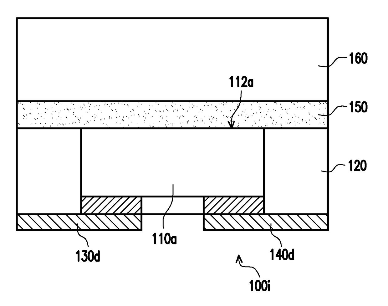
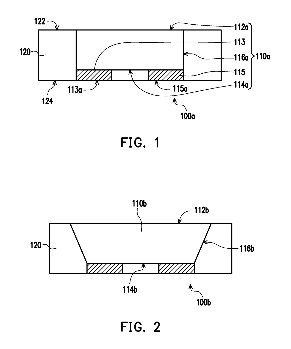
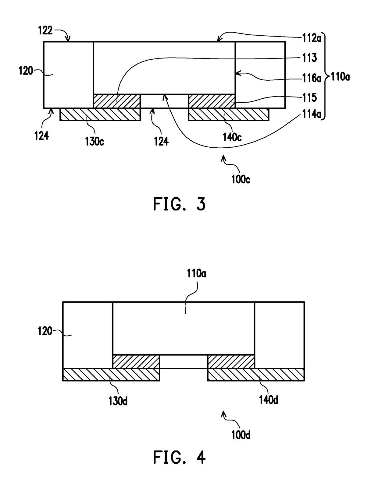
[0047]FIG. 1 shows a schematic of a light-emitting device of an embodiment of the invention. Referring first to FIG. 1, in the present embodiment, a light-emitting device 100a includes a light-emitting unit 110a and a reflective protecting element 120. The light-emitting unit 110a has an upper surface 112a and a lower surface 114a opposite to each other, a side surface 116a connected to the upper surface 112a and the lower surface 114a, and a first electrode pad 113 and a second electrode pad 115 located on the lower surface 114a and separated from each other. The reflective protecting element 120 covers the side surface 116a of the light-emitting unit 110a and exposes at least a portion of the upper surface 112a and at least a portion of a first bottom surface 113a of the first electrode pad 113 and at least a portion of a second bottom surface 115a of the second electrode pad 115.

[0048]More specifically, in the present embodiment, as shown in FIG. 1, the upper surface 112a of the ...


PUM


Abstract

A light-emitting device including at least one light-emitting unit, a wavelength conversion adhesive layer, and a reflective protecting element is provided. The light-emitting unit has an upper surface and a lower surface opposite to each other. The light-emitting unit includes two electrode pads, and the two electrode pads are located on the lower surface. The wavelength conversion adhesive layer is disposed on the upper surface. The wavelength conversion adhesive layer includes a low-concentration fluorescent layer and a high-concentration fluorescent layer. The high-concentration fluorescent layer is located between the low-concentration fluorescent layer and the light-emitting unit. The width of the high-concentration fluorescent layer is WH. The width of the low-concentration fluorescent layer is WL. The width of the light-emitting unit is WE. The light-emitting device further satisfies the following inequalities: WE<WL, WH<WL and 0.8<WH/WE≤1.2. Furthermore, a manufacturing method of the light-emitting device is also provided.

Description

CROSS-REFERENCE TO RELATED APPLICATION[0001]This application is a continuation-in-part application of and claims the priority benefit of U.S. application Ser. No. 15 / 268,654, filed on Sep. 19, 2016, now pending. This prior U.S. application Ser. No. 15 / 268,654 is a continuation-in-part application of and claims the priority benefit of U.S. application Ser. No. 14 / 711,798, filed on May 14, 2015, now pending, which claims the priority benefits of Taiwan application serial no. 103116987, filed on May 14, 2014 and U.S. provisional application Ser. No. 62 / 157,450, filed on May 5, 2015. This prior U.S. application Ser. No. 15 / 268,654 also claims the priority benefits of U.S. provisional application Ser. No. 62 / 220,249, filed on Sep. 18, 2015, U.S. provisional application Ser. No. 62 / 236,150, filed on Oct. 2, 2015, Taiwan application serial no. 105100499, filed on Jan. 8, 2016, U.S. provisional application Ser. No. 62 / 245,247, filed on Oct. 22, 2015, U.S. provisional application Ser. No. 62...

Claims


Application Information

Patent Timeline
Patent Type & Authority Applications(United States)
IPC IPC(8): H01L33/50H01L33/48H01L33/60H01L33/62H01L33/56
CPCH01L33/505H01L33/486H01L33/60H01L33/62H01L33/56H01L2933/0041H01L2933/0058H01L2933/005H01L33/508H01L33/54H01L2224/18H01L2933/0091
Inventor HUNG, CHENG-WEITU, LONG-CHICHANG, JUI-FUTSENG, CHUN-MINGCHEN, YUN-CHU
Owner GENESIS PHOTONICS
Why Eureka
Try Eureka