Method for identification of proper probe placement on printed circuit board

a technology of printed circuit boards and probes, applied in the field of printed circuit boards, can solve the problems of manual and error-prone probing process, translation errors can occur between signal integrity engineers and technicians doing the probing,

Inactive Publication Date: 2018-05-17
IBM CORP
View PDF1 Cites 10 Cited by
  • Summary
  • Abstract
  • Description
  • Claims
  • Application Information

AI Technical Summary

Problems solved by technology

Probing is a manual and error prone process involving comparison of PCB artwork on a computer to the physical PCB to find probe points.
Translation errors can occur between the signal integrity (SI) engineer and the technicians doing the probing.

Method used


Image

  • Method for identification of proper probe placement on printed circuit board
  • Method for identification of proper probe placement on printed circuit board
  • Method for identification of proper probe placement on printed circuit board

Examples


Embodiment Construction

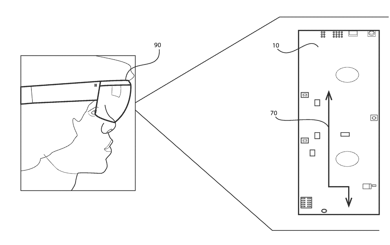
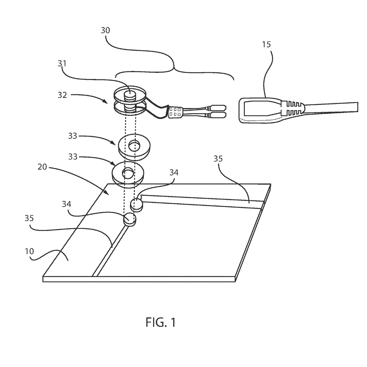
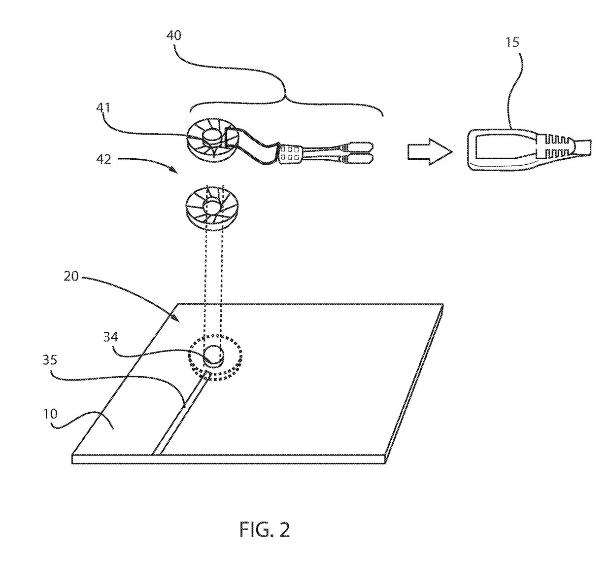
[0018]Detailed embodiments of the claimed structures and methods are disclosed herein; however, it is to be understood that the disclosed embodiments are merely illustrative of the claimed structures and methods that may be embodied in various forms. In addition, each of the examples given in connection with the various embodiments is intended to be illustrative, and not restrictive. Further, the figures are not necessarily to scale, some features may be exaggerated to show details of particular components. Therefore, specific structural and functional details disclosed herein are not to be interpreted as limiting, but merely as a representative basis for teaching one skilled in the art to variously employ the methods and structures of the present disclosure. For purposes of the description hereinafter, the terms “upper”, “lower”, “right”, “left”, “vertical”, “horizontal”, “top”, “bottom”, and derivatives thereof shall relate to the embodiments of the disclosure, as it is oriented i...


PUM


Abstract

A method of probing printed circuit boards that includes providing a circuit board design including a plurality of probe points, and selecting a probe point including a location ink from the plurality of probe points in the circuit board design to be probed on a physical printed circuit board design. The method continues with probing at least one probe point of the plurality of probe points with a probe that activates the location ink. Activation of the location ink by the probe indicates the selected probe point including the locating ink.

Description

BACKGROUNDTechnical Field[0001]The present disclosure relates generally to printed circuit boards (PCBs), and to preventing errors in probing printed circuit board for testing purposes when the user locates the probe point on the printed circuit board schematic and then goes to place the probe on the physical card.Description of the Related Art[0002]Electronic circuit boards for computers and other devices typically consist of many integrated circuits mounted on a printed circuit board (PCB). Individual integrated circuit (IC) packages have a semiconductor chip or die enclosed within a protective plastic package. A metal frame consisting of multiple conductive leads provides the electrical interconnect between the enclosed semiconductor chip and components exterior to the plastic package. The PCB has many conductive traces arranged on its surface according to a selected pattern for efficiently transferring electronic signals across the board to and from individual IC packages. Probi...

Claims


Application Information

Patent Timeline
Patent Type & Authority Applications(United States)
IPC IPC(8): G01R1/067G01R31/28G06T19/00
CPCG01R1/06794G06T19/006G01R31/2806G01R31/2801
Inventor ALBERT, JASON T.DOYLE, MATTHEW S.ENGEL, CHRISTOPHER J.EVANS, KAHN C.JANSSEN, STEVEN B.LIGHT, MATT K.
Owner IBM CORP
Why Eureka
Try Eureka