Pixel array

a pixel array and array technology, applied in the field of pixel arrays, can solve problems affecting display quality, and achieve the effect of reducing the number of conductive structures required for conducting through the common electrodes and insufficient aperture ratio of the pixel array

Active Publication Date: 2018-11-15
AU OPTRONICS CORP
View PDF0 Cites 1 Cited by
  • Summary
  • Abstract
  • Description
  • Claims
  • Application Information

AI Technical Summary

Benefits of technology

[0005]The invention is directed to a pixel array, which is capable of solving the problem of the aperture ratio restricted by the conductive structures.
[0007]Based on the above, in the pixel array of the invention, the first pixel unit has the first conductive structure, and the second pixel unit has the second conductive structure. Because the second common electrode of the first pixel unit can be electrically connected to the third common electrode of the second pixel unit simply through two conductive structures and the first signal line, the number of conductive structures required for conducting through the common electrodes may be reduced accordingly. In this way, the problem regarding the insufficient aperture ratio of the pixel array can be solved.

Problems solved by technology

Consequently, an aperture ratio of the pixel array is restricted thereby affecting the display quality.

Method used


Image

  • Pixel array
  • Pixel array
  • Pixel array

Examples


Embodiment Construction

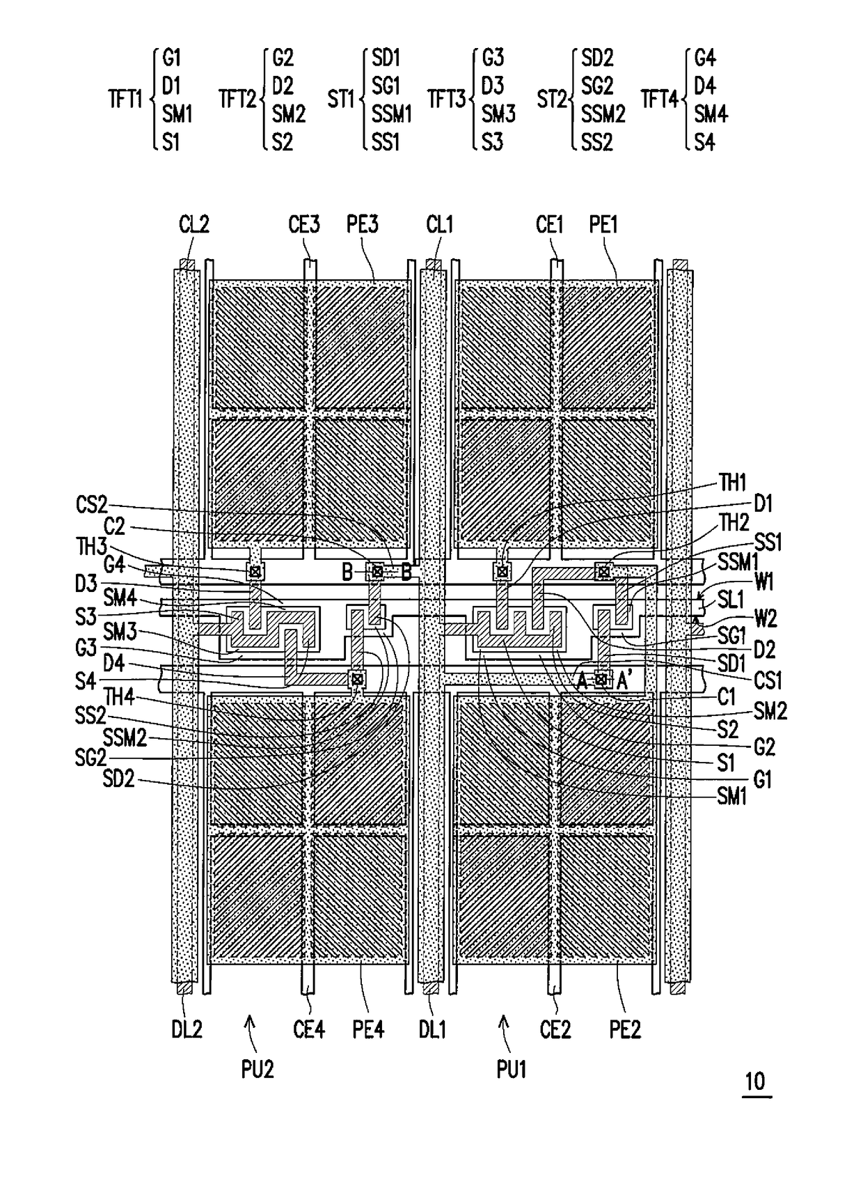
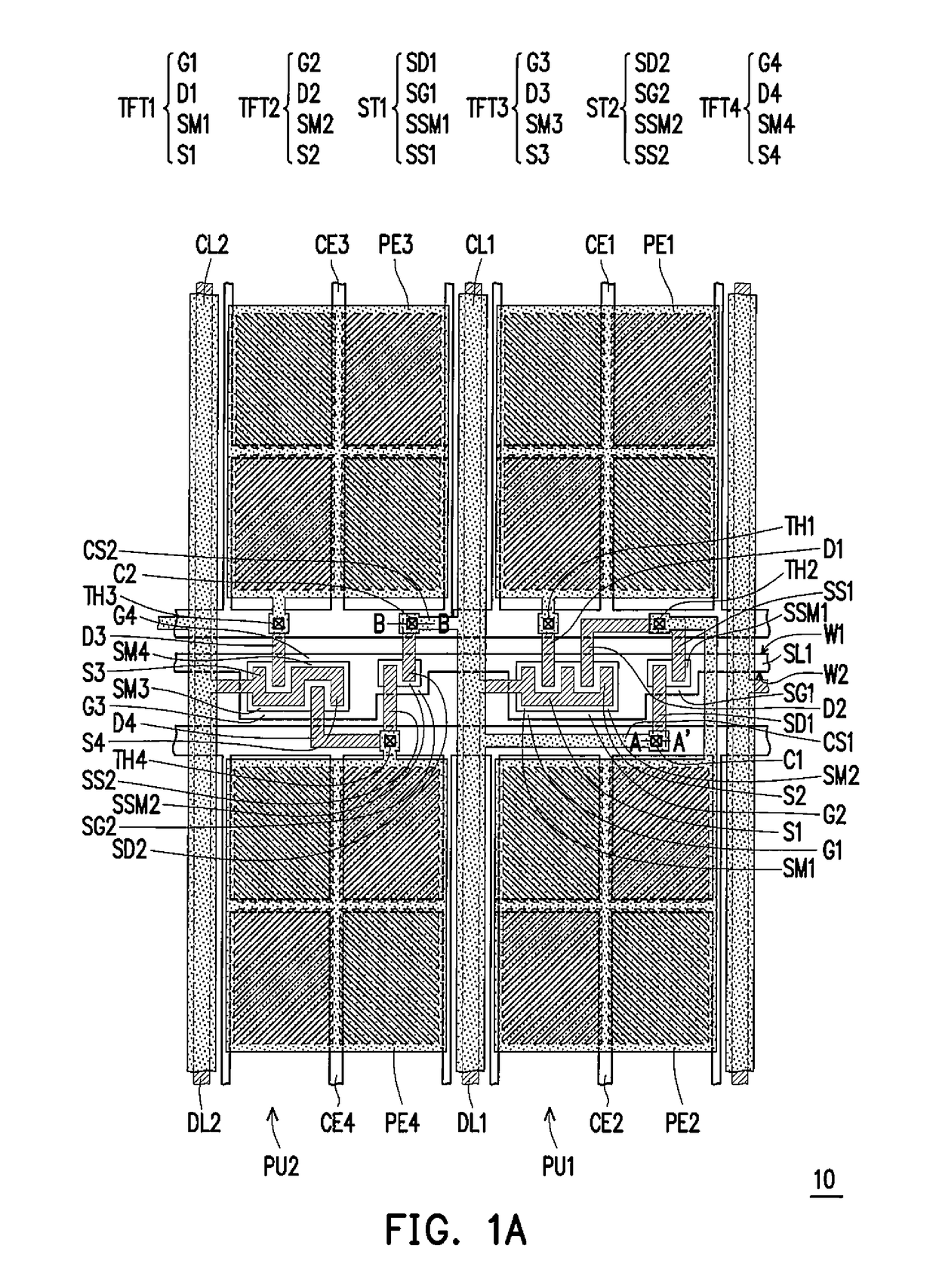
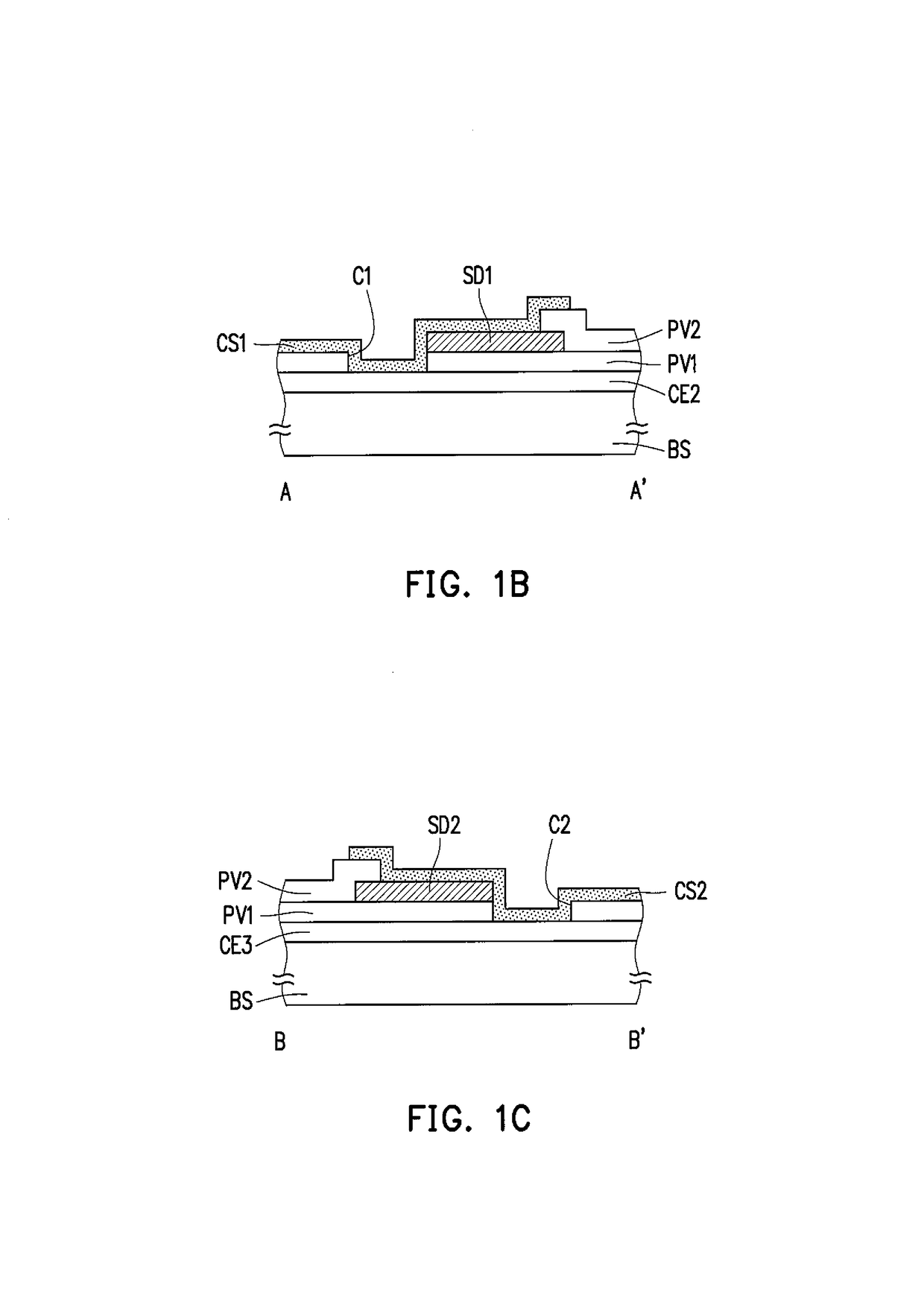
[0017]Reference will now be made in detail to the present preferred embodiments of the invention, examples of which are illustrated in the accompanying drawings. Wherever possible, the same reference numbers are used in the drawings and the description to refer to the same or like parts.

[0018]The following describes the embodiments with reference to the accompanying drawings in detail, so as to make the aspects of the present disclosure more comprehensible. However, the mentioned embodiments are not intended to limit the scope of the present disclosure, and the description of the operation of a structure is not intended to limit an execution sequence. Any device with equivalent functions that is produced from a structure formed by a recombination of elements shall fall within the scope of the present disclosure. Besides, according to industry standards and practices, the drawings are merely intended to assist the description, and are not drawn according to original dimensions. In pr...


PUM


Abstract

A pixel array including a first scan line, a first data line, a first signal line, a first pixel unit, and a second pixel unit is provided. The first pixel unit includes a first common electrode and a second common electrode. The first common electrode and the second common electrode are respectively located on a first side and a second side of the first scan line. The second common electrode is electrically connected to the first signal line through a first conductive structure. The second pixel unit includes a third common electrode and a fourth common electrode. The third common electrode and the fourth common electrode are respectively located on the first side and the second side of the first scan line. The third common electrode is electrically connected to the first signal line through a second conductive structure.

Description

CROSS-REFERENCE TO RELATED APPLICATION[0001]This application claims the priority benefit of Taiwan application serial no. 106115227, filed on May 9, 2017. The entirety of the above-mentioned patent application is hereby incorporated by reference herein and made a part of this specification.BACKGROUND OF THE INVENTION1. Field of the Invention[0002]The invention relates to a pixel array, and more particularly, to a pixel array having a conductive structure.2. Description of Related Art[0003]In recent years, with the continuous progress of display technology, viewer's demand on a display quality (e.g., image resolution, color saturation, etc.) of a display also becomes increasingly higher. Yet, in order to manufacture a display with high performance, a pixel array in the display needs to include conductive structures connecting different conductive layers.[0004]In the pixel array, a great portion of area is occupied by the conductive structures connecting the different conductive layer...

Claims


Application Information

Patent Timeline
Patent Type & Authority Applications(United States)
IPC IPC(8): H01L27/12H01L27/32
CPCH01L27/124H01L27/32G02F2201/123G09G2300/0426G02F2201/121G02F1/136227G02F1/13624G02F1/136286G02F1/1368H10K59/1213H10K59/131H10K59/00
Inventor WANG, JIA-HONGHSU, YA-LINGLIAO, CHEN-HSIEN
Owner AU OPTRONICS CORP
Why Eureka
Try Eureka