Semiconductor Structure with Layer Having Protrusions

Active Publication Date: 2019-08-29
SENSOR ELECTRONICS TECH
View PDF8 Cites 2 Cited by
  • Summary
  • Abstract
  • Description
  • Claims
  • Application Information

AI Technical Summary

Benefits of technology

The invention provides a layer with raised areas on its surface that can improve the properties of semiconductor layers and optoelectronic devices made from them. These raised areas are separated by a smooth surface. They can contain gas or different materials, and help to make the layer more suitable for use in different applications.

Problems solved by technology

Changes in molar fractions of semiconductor alloys can allow for band gap control, but can lead to abrupt changes in the optical properties of the materials and result in light trapping.
A small TIR angle results in a large fraction of light rays reflecting from the interface boundaries, thereby leading to light trapping and subsequent absorption by the semiconductor layers and / or LED metal contacts.
Nevertheless, light only can be partially transmitted through the interface, even if it does not undergo TIR, due to Fresnel losses.

Method used


Image

  • Semiconductor Structure with Layer Having Protrusions
  • Semiconductor Structure with Layer Having Protrusions
  • Semiconductor Structure with Layer Having Protrusions

Examples


Embodiment Construction

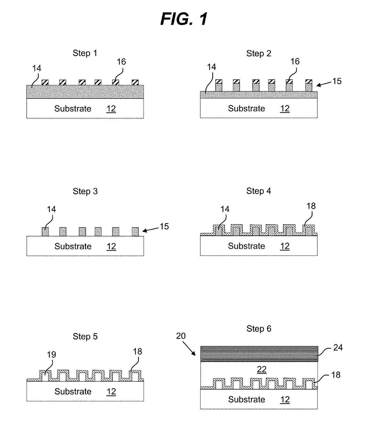
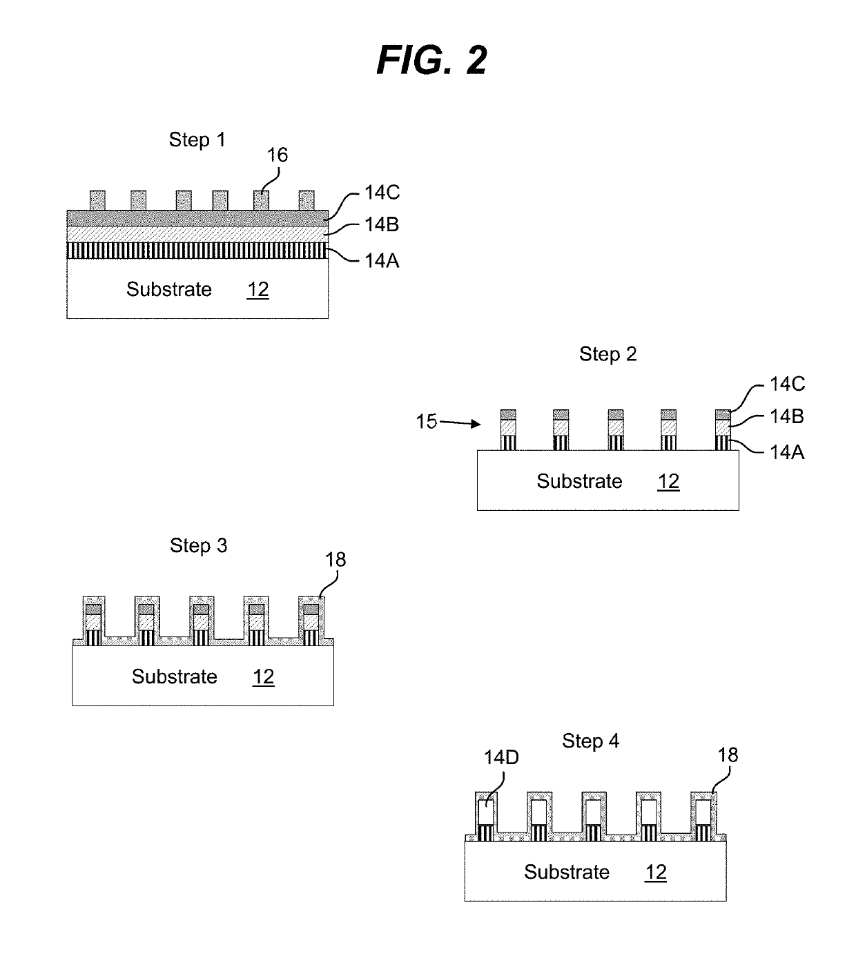
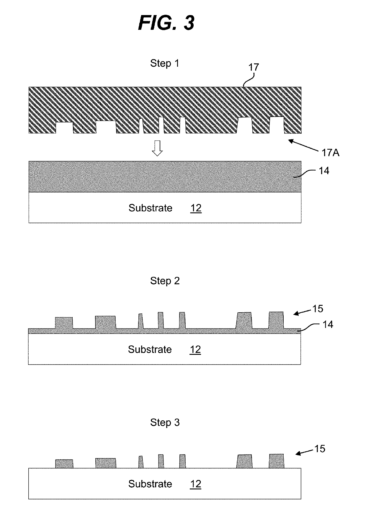
[0025]As indicated above, aspects of the invention provide a growth layer having a growth surface with protruding domains. The growth layer can improve one or more attributes of the semiconductor layer(s) grown thereon and / or one or more attributes of an optoelectronic device fabricated from the semiconductor heterostructure. The protruding domains can be separated by a substantially flat growth surface located between the protruding domains. A protruding domain can include an internal region that can be filled with a gas and / or can be partially or completely filled with one or more materials that differ from the material of the growth layer, which forms an outer surface of each of the protruding domains.

[0026]It is understood that, unless otherwise specified, each value is approximate and each range of values included herein is inclusive of the end values defining the range. As used herein, unless otherwise noted, the term “approximately” is inclusive of values within + / − ten perce...


PUM


Abstract

A growth layer having a growth surface with protruding domains is described. The protruding domains can be separated by a substantially flat growth surface located between the protruding domains. A protruding domain can include an internal region that can be filled with a gas and / or can be partially or completely filled with one or more materials that differ from the material of the growth layer, which forms an outer surface of each of the protruding domains.

Description

REFERENCE TO RELATED APPLICATIONS[0001]The current application claims the benefit of U.S. Provisional Application No. 62 / 636,835, filed on 28 Feb. 2018, which is hereby incorporated by reference.TECHNICAL FIELD[0002]The disclosure relates generally to semiconductor structures, and more particularly, to a semiconductor structure including one or more layers with protrusions.BACKGROUND ART[0003]Semiconductor structures are fabricated as part of the manufacture of various types of semiconductor devices, including optoelectronic devices. Optoelectronic devices include semiconductor emitting devices, such as light emitting diodes (LEDs) and laser diodes (LDs), which can be solid state emitting devices composed of group III-V semiconductors. A subset of group III-V semiconductors includes group III nitride alloys, which can include binary, ternary and quaternary alloys of indium (In), aluminum (Al), gallium (Ga), and nitrogen (N). Illustrative group III nitride based LEDs and LDs can be o...

Claims


Application Information

Patent Timeline
IPC IPC(8): H01L33/22H01L33/32H01L33/00
CPCH01L33/22H01L33/002H01L33/007H01L33/32H01L33/025H01L2933/0091H01L21/7806
Inventor GAEVSKI, MIKHAILDOBRINSKY, ALEXANDER
Owner SENSOR ELECTRONICS TECH
Why Eureka
Try Eureka