Anisotropic conductive adhesive bond in a piezoelectric micro-electro-mechanical system scanning mirror system

a micro-electromechanical system and anisotropic technology, applied in the field of anisotropic conductive adhesive bond in the piezoelectric micro-electromechanical system scanning mirror system, can solve the problems of insufficient conductive material and insufficient compressed adhesive out of the bond line, so as to achieve maximum mechanical and electrical performance, improve system efficiency and life, and sparse loading of conductive particles

Active Publication Date: 2020-11-19
MICROSOFT TECH LICENSING LLC
View PDF0 Cites 0 Cited by
  • Summary
  • Abstract
  • Description
  • Claims
  • Application Information

AI Technical Summary

Benefits of technology

[0005]Aspects of the present invention relate to piezoelectric MEMS scanning mirror systems. In particular, the efficiency and life of the system are improved by use of new bonding methods. For example, aspects of the present invention relate to creating mechanical and electrical connections between the actuator frame of a piezoelectric MEMS scanning mirror system and the piezoelectric actuators in the system using an anisotropic conductive adhesive. An anisotropic conductive adhesive only conducts electricity across the bond line between a lower portion of the piezoelectric actuator and a top of the metal frame. One way this is done is to provide a sparse loading of conductive particles. When the piezoelectric element is compressed against the frame, the conductive particles only form a conductive path across the bond line. Adhesive that is squeezed out of the bond line is not compressed and does not have sufficient conductive material to form a path from the frame to the top electrode on the piezoelectric element. The result is a system with maximum mechanical and electrical performance and increased efficiency.
[0006]The bond between the metal frame and the MEMS resonance mirror is a highly stressed bond and critical to the performance of the device. The initial and long term strength of this bond may be improved by roughening the metal frame surface to increase the bond surface area. Grit blasting, sanding, or chemical etching may be used to roughen the metal surface prior to bonding. In one aspect, a surface roughness between 2 RMS and 6 RMS is created on the metal frame.

Problems solved by technology

Adhesive that is squeezed out of the bond line is not compressed and does not have sufficient conductive material to form a path from the frame to the top electrode on the piezoelectric element.

Method used


Image

  • Anisotropic conductive adhesive bond in a piezoelectric micro-electro-mechanical system scanning mirror system
  • Anisotropic conductive adhesive bond in a piezoelectric micro-electro-mechanical system scanning mirror system
  • Anisotropic conductive adhesive bond in a piezoelectric micro-electro-mechanical system scanning mirror system

Examples


Embodiment Construction

[0023]The subject matter of the present disclosure is described with specificity herein to meet statutory requirements. However, the description itself is not intended to limit the scope of this patent. Rather, the inventors have contemplated that the claimed subject matter might also be embodied in other ways, to include different steps or combinations of steps similar to the ones described in this document, in conjunction with other present or future technologies. Moreover, although the terms “step” and / or “block” may be used herein to connote different elements of methods employed, the terms should not be interpreted as implying any particular order among or between various steps herein disclosed unless and except when the order of individual steps is explicitly described. As used herein, the singular forms “a,”“an,” and “the” are intended to include the plural forms as well, unless the context clearly indicates otherwise.

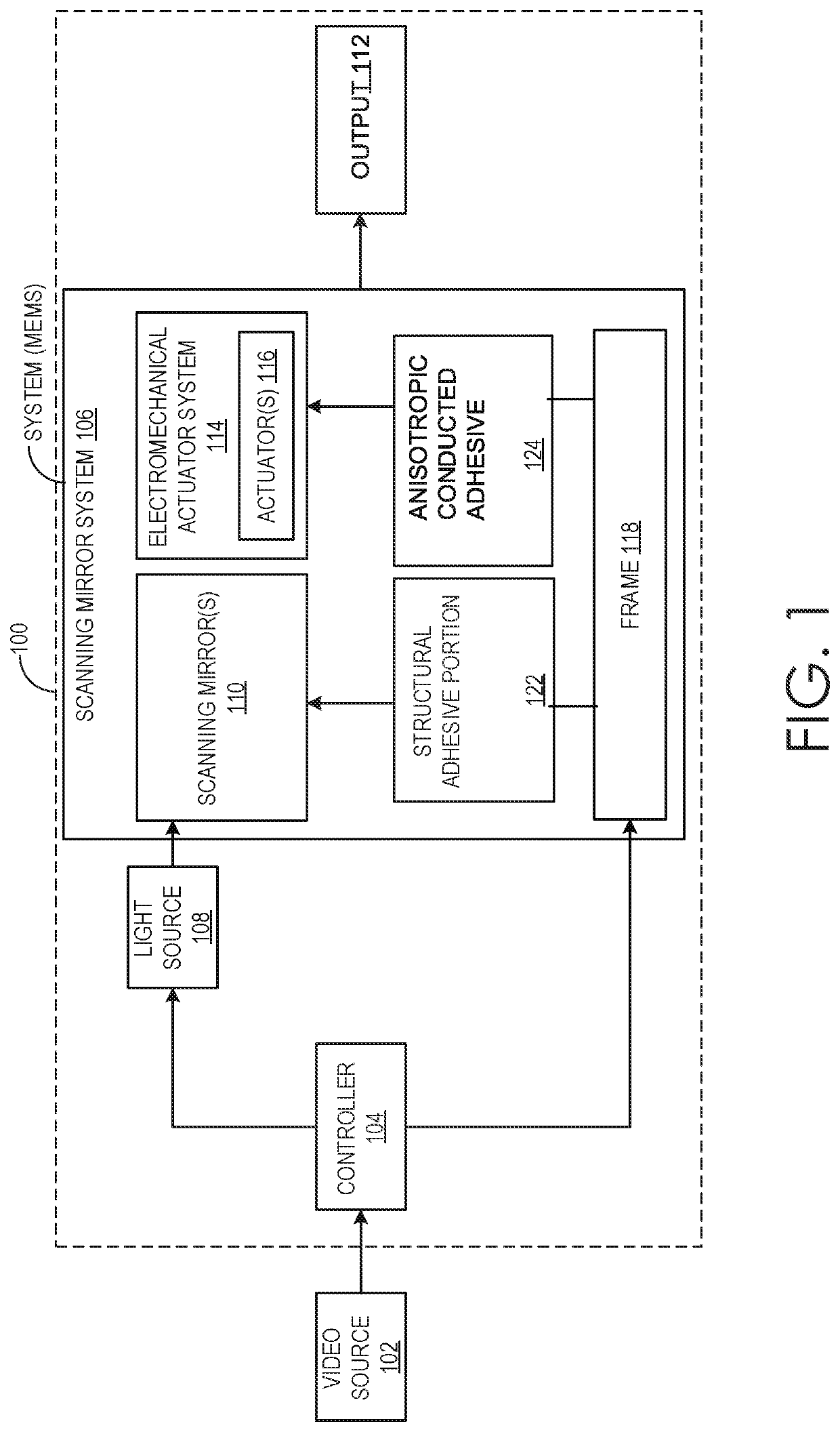
[0024]Aspects of the present invention relate to piezoelec...


PUM

PropertyMeasurementUnit
thickaaaaaaaaaa
electrically conductiveaaaaaaaaaa
anisotropic conductiveaaaaaaaaaa

Abstract

A piezoelectric MEMS scanning mirror system is provided. In particular, the efficiency and life of the system are improved by use of new bonding methods. Mechanical and electrical connections between the actuator frame of a piezoelectric MEMS scanning mirror system and the piezoelectric actuators in the system may be created using an anisotropic conductive adhesive. An anisotropic conductive adhesive only conducts electricity across the bond line between a lower portion of the piezoelectric actuator and a top of the metal frame. One way this is done is to provide a sparse loading of conductive particles. When the piezoelectric element is compressed against the frame, the conductive particles only form a conductive path across the bond line. Grit blasting, sanding, or chemical etching may be used to roughen the metal surface prior to bonding. A surface roughness between 2 RMS and 6 RMS may be created on the metal frame.

Description

BACKGROUND[0001]In traditional piezoelectric micro-electro-mechanical system (MEMS) scanning mirror systems, a metal frame acts as the common mechanical and electrical connection for all of the piezoelectric elements. Various components of the system are bonded to the frame. These bonds represent potential failure points in the system. Improving the system bonds can improve the life of the piezoelectric MEMS scanning mirror systems.[0002]In these devices, the frame serves as one electrical connection to the bottom electrode of the piezoelectric element, and a wire serves as the electrical connection to the top electrode of the piezoelectric element. The adhesive that forms the bond between the frame and the bottom electrode must have some electrical conductivity for the device to function. In a typical application, a conductive adhesive would be used. In addition, for efficient and uniform transfer of the mechanical force, adhesive must completely fill the bond line between the fram...

Claims


Application Information

Patent Timeline
Patent Type & Authority Applications(United States)
IPC IPC(8): G02B26/08H02N2/02H02N2/00G02B26/10
CPCG02B26/101H02N2/0085G02B26/0858H02N2/028G02B26/105C09J9/02H01B1/20B81C3/001
Inventor LUIZZI, JOSEPH MICHAELNYSTROM, MICHAEL JAMES
Owner MICROSOFT TECH LICENSING LLC
Why Eureka
Try Eureka