Display Device
a display device and display line technology, applied in the field of display devices, can solve the problems of insufficient space in the bezel area in which display link lines are connected to display lines and touch lines, and it is difficult to reduce the width of the bezel area, so as to achieve the effect of reducing the bezel area
- Summary
- Abstract
- Description
- Claims
- Application Information
AI Technical Summary
Benefits of technology
Problems solved by technology
Method used
Image

Examples
first embodiment
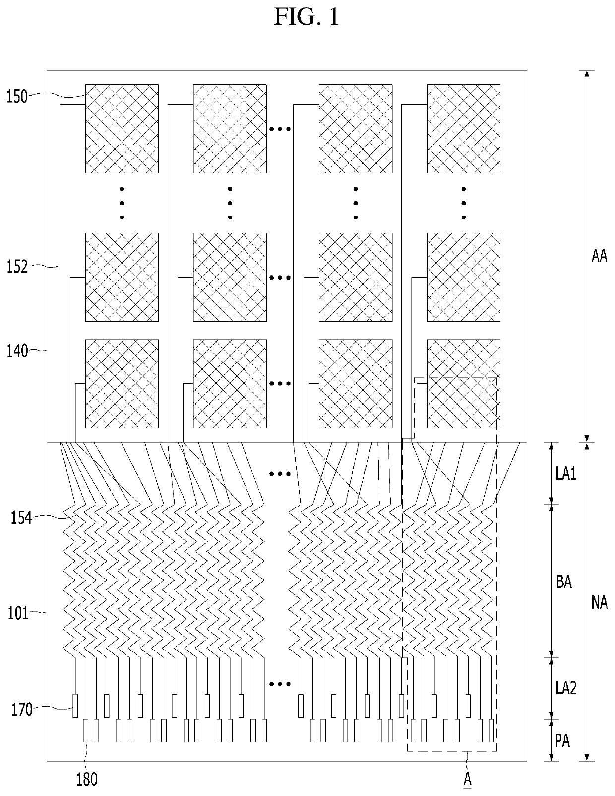
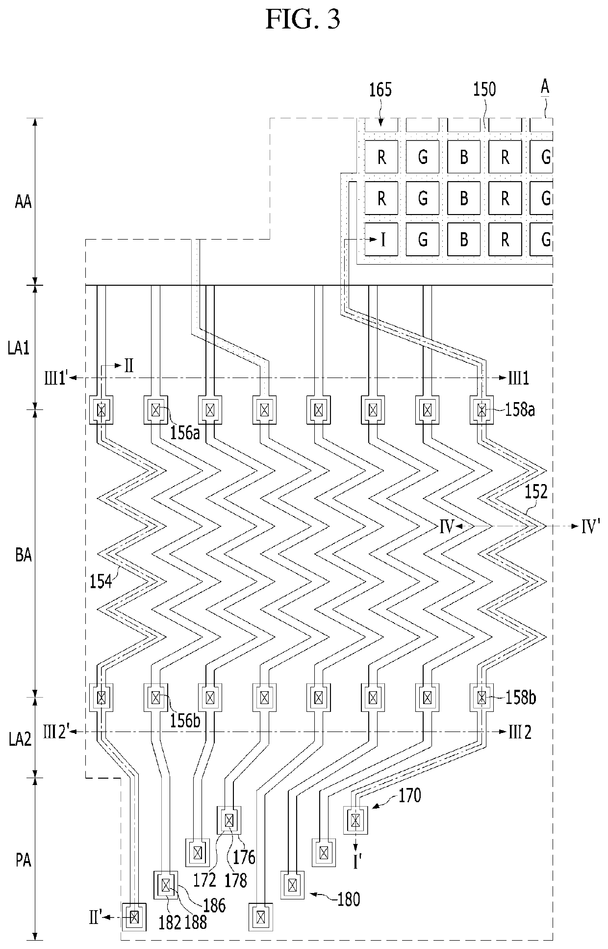
[0023]FIG. 1 is a plan view showing a display device according to the present disclosure.
[0024]The display device shown in FIG. 1 is divided into an active area AA and a non-active area NA provided on a substrate 101.
[0025]A plurality of display elements and a plurality of touch electrodes 150 are disposed in the active area AA. Each of the plurality of touch electrodes 150 includes capacitance formed therein and thus is used as a self-capacitance touch sensor configured to sense a change in capacitance due to user touch. In a self-capacitance sensing method using such a touch electrode 150, electric charge is accumulated in a touch sensor when a drive signal supplied through a touch line 152 is applied to the touch electrode 150. At this time, when a user's finger or a conductive object contacts the touch electrode 150, parasitic capacitance is additionally connected to a self-capacitance sensor, whereby the value of capacitance is changed. Consequently, the value of capacitance of...
second embodiment
[0100]FIG. 9 is a sectional view showing a display device according to the present disclosure.
[0101]The display device shown in FIG. 9 includes the same components as the display device shown in FIG. 4 except that an adhesive reinforcement layer 198 is further included. Consequently, a detailed description of the same components will be omitted.
[0102]The adhesive reinforcement layer 198 is disposed between the crack prevention layer 148 and each of the touch line 152, the third touch pad electrode 176, and the third display pad electrode 186. The adhesive reinforcement layer 198 is formed so as to include indium having high adhesive strength with a conductive layer (e.g. Ti) included in each of the touch line 152, the third touch pad electrode 176, and the third display pad electrode 186 and an organic film included in the crack prevention layer 148. For example, the adhesive reinforcement layer 198 may be made of the same material as the anode 122, including an IZO- or IGZO-based m...
third embodiment
[0109]FIG. 10 is a sectional view showing an organic light-emitting display device having a touch sensor according to the present disclosure.
[0110]The organic light-emitting display device having the touch sensor shown in FIG. 10 includes the same components as the organic light-emitting display device shown in FIG. 4 except that a color filter array 190 is further included. Consequently, a detailed description of the same components will be omitted.
[0111]The color filter array 190 includes a color filter 196, a black matrix 194, and a touch planarization film 192 disposed on the encapsulation unit 140.
[0112]The color filter 196 is disposed so as to overlap each of the subpixels R, G, and B. In the case in which the light-emitting layer included in the light-emitting stack 124 emits white light, the color filter 196 is disposed on the encapsulation unit 140. In the case in which the light-emitting layer included in the light-emitting stack 124 emits red, green, or blue light corresp...
PUM
| Property | Measurement | Unit |
|---|---|---|
| distance | aaaaa | aaaaa |
| area | aaaaa | aaaaa |
| non-active area | aaaaa | aaaaa |
Abstract
Description
Claims
Application Information
 - R&D Engineer
- R&D Manager
- IP Professional
- Industry Leading Data Capabilities
- Powerful AI technology
- Patent DNA Extraction
Browse by: Latest US Patents, China's latest patents, Technical Efficacy Thesaurus, Application Domain, Technology Topic.
© 2024 PatSnap. All rights reserved.Legal|Privacy policy|Modern Slavery Act Transparency Statement|Sitemap