
Apparatus for cleaning semiconductor substrates

Active Publication Date: 2021-05-13
ACM RES SHANGHAI
View PDF1 Cites 0 Cited by
  • Summary
  • Abstract
  • Description
  • Claims
  • Application Information

AI Technical Summary

Benefits of technology

The present invention is an apparatus for cleaning semiconductor substrates that prevents corrosion of sulfuric acid fume to parts in the cleaning chamber. It has two purposes: to improve safety in the manufacture of semiconductor devices and to use hot SPM cleaning in a sealed chamber to prevent acid fume from coroding parts in the chamber. After the cleaning process is completed, the temperature of the seal room cools down, and the enclosing wall moves down to allow the external dispenser or ultrasonic device to get in and process the semiconductor substrate. This ensures secure use of IPA.

Problems solved by technology

Correspondingly, the demand to substrate surface cleanliness becomes much stricter because poor clean may cause device failure which will increase the cost of integrated circuit manufacture.
Although completely clean substrate surface is not present, however, the development of VLSI requires the substrate surface to be as clean as possible, which makes the substrate cleaning process face challenges.
Such high concentration and high temperature will generate sulfuric acid fume.
Due to lack of effective processing of the sulfuric acid fume, the use of SPM is limited and the SPM cleaning cannot be widely popularized.
In a conventional substrate cleaning apparatus, high temperature sulfuric acid fume may fill a cleaning chamber of the substrate cleaning apparatus, causing corrosion of the sulfuric acid fume to parts in the cleaning chamber.
Therefore, the use of high temperature SPM in the conventional substrate cleaning apparatus poses a serious threat to the production safety.

Method used


Image

  • Apparatus for cleaning semiconductor substrates
  • Apparatus for cleaning semiconductor substrates
  • Apparatus for cleaning semiconductor substrates

Examples


Embodiment Construction

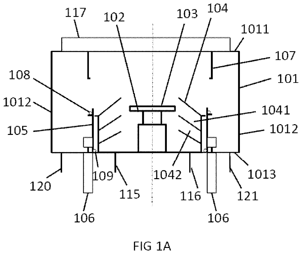
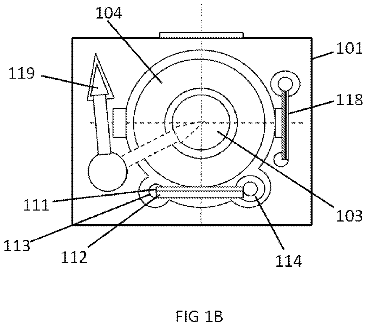
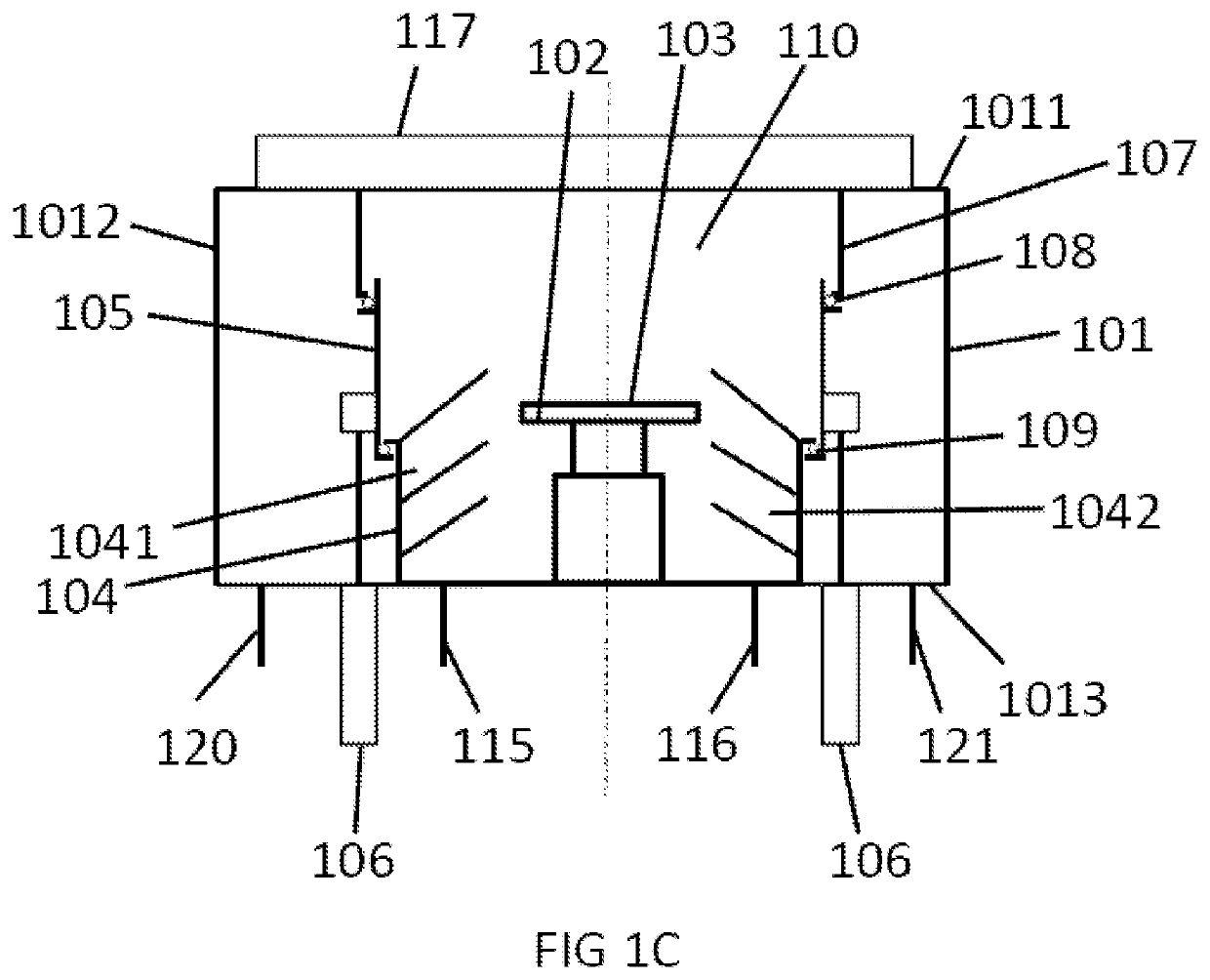
[0013]Referring to FIG. 1A to FIG. 1D, an apparatus for cleaning semiconductor substrates according to an embodiment of the present invention is illustrated. The apparatus has a chamber 101. The chamber 101 has a top wall 1011, a side wall 1012 and a bottom wall 1013. Generally, the side wall 1012 of the chamber 101 has an opening for transferring a semiconductor substrate 103. The opening is commonly sealed by a door which is controlled to open or close. A chuck 102 is positioned in the chamber 101 for holding the semiconductor substrate 103. The chuck 102 is driven to rotate by a rotating driving device. The semiconductor substrate 103 rotates along with the chuck 102. A liquid collector 104 surrounds the chuck 102. The liquid collector 104 has at least one annular tilted trough to have spun off liquid collected therein. As an example, the liquid collector 104 has two annular tilted troughs 1041, 1042. Every annular tilted trough 1041, 1042 is connected to a pipe (not shown) throu...


PUM


Abstract

An apparatus for cleaning semiconductor substrates includes a chamber (101), a chuck (102), a liquid collector (104), an enclosing wall (105), at least one driving mechanism (106), at least one internal dispenser (111), and at least one external dispenser (118). The chamber (101) has a top wall (1011), a side wall (1012) and a bottom wall (1013). The chuck (102) is disposed in the chamber (101) for holding a semiconductor substrate (103). The liquid collector (104) surrounds the chuck (102). The enclosing wall (105) surrounds the liquid collector (104). The at least one driving mechanism (106) drives the enclosing wall (105) to move up and down, wherein when the at least one driving mechanism (106) drives the enclosing wall (105) to move up, a seal room (110) is formed by the liquid collector (104), the enclosing wall (105), the top wall (1011) of the chamber (101), and the bottom wall (1013) of the chamber (101). The at least one internal dispenser (111) is disposed inside the seal room (110). The at least one external dispenser (118) is disposed outside the seal room (110). The at least one external dispenser (118) gets in and out the seal room (110) after the enclosing wall (105) is driven to move down.

Description

BACKGROUND OF THE INVENTION1. Field of the Invention[0001]The present invention generally relates to the field of semiconductor devices manufacture, and more particularly to an apparatus for cleaning semiconductor substrates, which prevents corrosion of acid or alkali fume to parts in a cleaning chamber of the apparatus.2. The Related Art[0002]With the development of semiconductor industry, the feature size of semiconductor devices is continuously decreasing and the integration of chips is increasing. Correspondingly, the demand to substrate surface cleanliness becomes much stricter because poor clean may cause device failure which will increase the cost of integrated circuit manufacture. For obtaining high quality semiconductor devices, the substrates must have a very clean surface, which means there are no particles, metal, organic, etc. pollutants. Although completely clean substrate surface is not present, however, the development of VLSI requires the substrate surface to be as ...

Claims


Application Information

Patent Timeline
IPC IPC(8): B08B3/12H01L21/02
CPCB08B3/12B08B2240/00H01L21/02041H01L21/76H01L21/67051H01L21/67126H01L21/67098H01L21/67259
Inventor WANG, HUITAO, XIAOFENGCHEN, FUPINGJIA, SHENAWANG, XIZHANG, XIAOYANLI, XUEJUN
Owner ACM RES SHANGHAI
Learn More