Unlock instant, AI-driven research and patent intelligence for your innovation.

Circuit board

a technology of circuit boards and components, applied in the direction of printed circuit parts, coupling device connections, printed circuit manufacturing, etc., can solve the problems of easy damage of mating contacts, achieve the effect of reducing friction coefficient, reducing the size of circuit boards, and suppressing damage to front end portions or mating contacts

Active Publication Date: 2022-02-17
TYCO ELECTRONICS JAPAN GK
View PDF1 Cites 0 Cited by
  • Summary
  • Abstract
  • Description
  • Claims
  • Application Information

AI Technical Summary

Benefits of technology

The patent text describes various ways to protect electronic components from damage during assembly and use. One way is to use a protective film that can slid over pads on a base body to prevent damage to the pads. The protective film can be formed on both surfaces of the base body, allowing for smaller circuit boards. Additionally, the front end of the base body can be tapered to help with smooth mating with mating connectors and to prevent damage to the front end. The protective film can also have a low friction coefficient for easy insertion and extraction. These methods can help to make assembly more efficient and protect components from damage during use.

Problems solved by technology

When the edge, at the front end in the sliding direction, of the pad is pointed forward, the mating contact may contact the pointed front end having a narrow width in riding over the pad, whereby the mating contact is easily damaged.

Method used


Image

  • Circuit board
  • Circuit board
  • Circuit board

Examples


Embodiment Construction

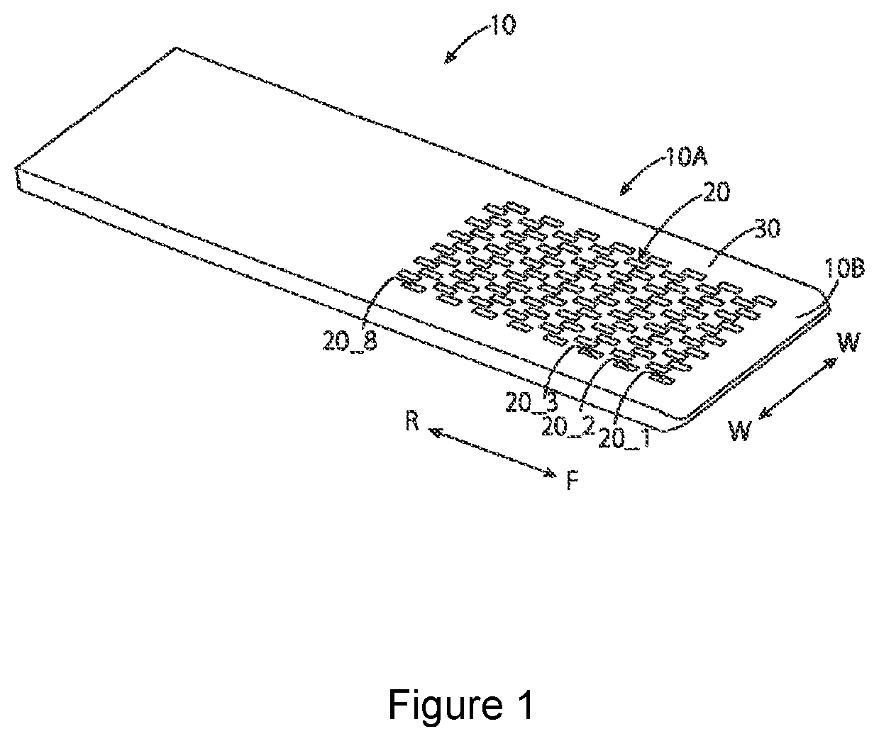
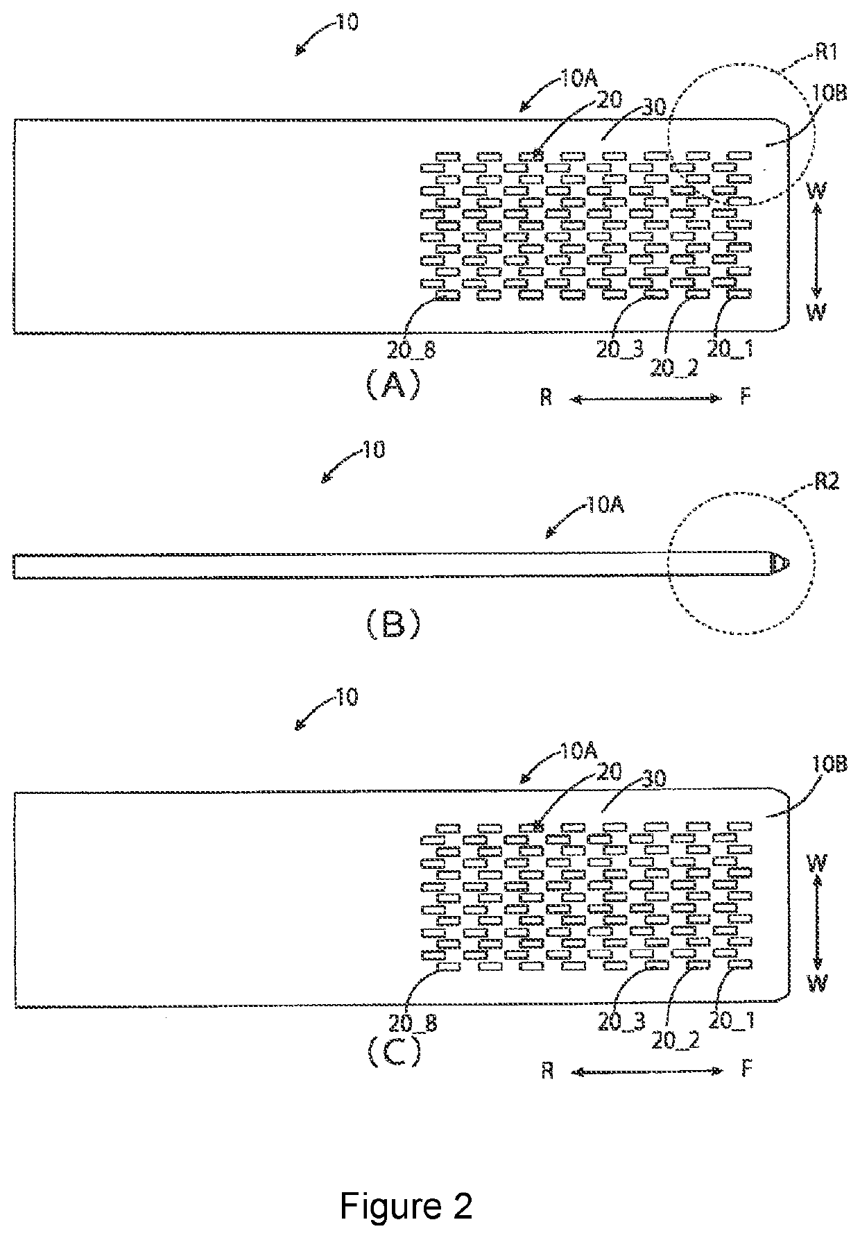
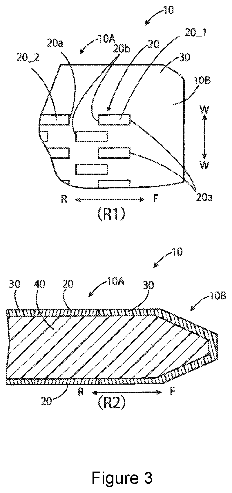
[0021]FIG. 1 is an isometric view of a circuit board 10 in accordance with an exemplary embodiment. FIG. 2 is a top view (A), a side view (B), and a bottom view (C) of the circuit board 10 in accordance with an exemplary embodiment. In FIG. 1 and FIG. 2, illustration of elements other than elements characteristic of the present embodiment on the circuit board is omitted. Description of the elements the illustration of which is omitted is also omitted.

[0022]In the circuit board 10, many pads 20 are arranged on both its front surface (see FIG. 2 (A) and rear surface (see FIG. 2 (B)). Thus, when the pads 20 are formed on both the front surface and the rear surface of the circuit board 10, more pads 20 can be positioned, as compared with when pads 20 are formed on only one of the surfaces. If the number of pads 20 is the same, the circuit board 10 can be miniaturized.

[0023]The many pads 20 illustrated in FIG. 1 and FIG. 2 are pads responsible for electrical contact with a mating contact...


PUM


Abstract

A circuit board includes a protective film of such a type that a mating contact slides on the protective film and rides over a pad, and is prevented from deteriorating due to attachment and detachment. A circuit board 10 includes a plate-shaped base body 40, a pad 20 formed on a surface of the base body 40 and responsible for electrical contact with a mating contact, and a protective film 30 that spreads on the surface of the base body 40 in contact with an edge of the pad 20. The edge of the pad 20 and a portion, which contacts the edge of the pad 20, of the protective film 30 respectively have heights consecutive to each other. The pad 20 contacts, by causing the mating contact that has slid in a sliding direction in contact with the protective film 30 to ride over the pad 20, the mating contact that has ridden over the pad 20.

Description

CROSS REFERENCE TO RELATED APPLICATIONS[0001]This application claims priority to JP Application No. 2020-136680, filed Aug. 13, 2020, the subject matter of which is herein incorporated by reference in its entirety.BACKGROUND[0002]The subject matter herein relates generally to a circuit board appropriate for a card edge connector.[0003]A card edge connector using an electrically conductive pad formed in a circuit board as a contact that electrically contacts a mating contact provided in a connector as a mating counterpart. For example, Japanese Patent JP3894774B discloses a card edge connector in which a protective pad is formed on the side of a front end, toward which a mating contact slides in mating, of an electrically conductive pad responsible for contact with the mating contact.[0004]A protective film called a resist is often formed in a circuit board. A pad responsible for electrical conduction is often formed in a circuit board. For example, in the case of a card edge connect...

Claims


Application Information

Patent Timeline
Patent Type & Authority Applications(United States)
IPC IPC(8): H05K1/11H01R12/72
CPCH05K1/117H05K2201/098H05K2201/09145H01R12/721H05K1/111H05K1/02H05K2203/1377H05K2201/09881H05K3/285H05K2201/09154H05K2201/09409H05K2201/09709
Inventor KIMURA, MAKIYAYAMAGA, SATOSHISASAKI, YOHICHI
Owner TYCO ELECTRONICS JAPAN GK