Memory test circuit

Active Publication Date: 2022-05-05
ELITE SEMICON MEMORY TECH INC
View PDF0 Cites 0 Cited by
  • Summary
  • Abstract
  • Description
  • Claims
  • Application Information

AI Technical Summary

Benefits of technology

The present invention provides a memory test circuit that can automatically identify the type of error that occurred. This eliminates the need for a lot of time and effort to confirm the error type. The circuit provides reference information that helps to quickly identify the error type.

Problems solved by technology

However, in the FT mode, the memory can only store a very small number of addresses for word lines with errors, that is, only a very small number of redundant word lines can be used.
However, when the memory has errors, it may be caused by other reasons besides the number of addresses for word lines with errors is greater than the number of word line error addresses that can be stored.
In the current memory test method, when the memory has an error, it needs a lot of efforts and time to confirm the type of error.

Method used


Image

  • Memory test circuit
  • Memory test circuit
  • Memory test circuit

Examples


Embodiment Construction

[0011]Several embodiments are provided in following descriptions to explain the concept of the present invention. Each component in following descriptions can be implemented by hardware (e.g. a device or a circuit) or hardware with software (e.g. a program installed to a processor). It will be understood that, although the terms first, second, third, etc. may be used herein to describe various elements, these elements should not be limited by these terms. These terms may be used to distinguish one element from another. For example, a first element may be termed a second element and a second element may be termed a first element without departing from the scope of the present invention.

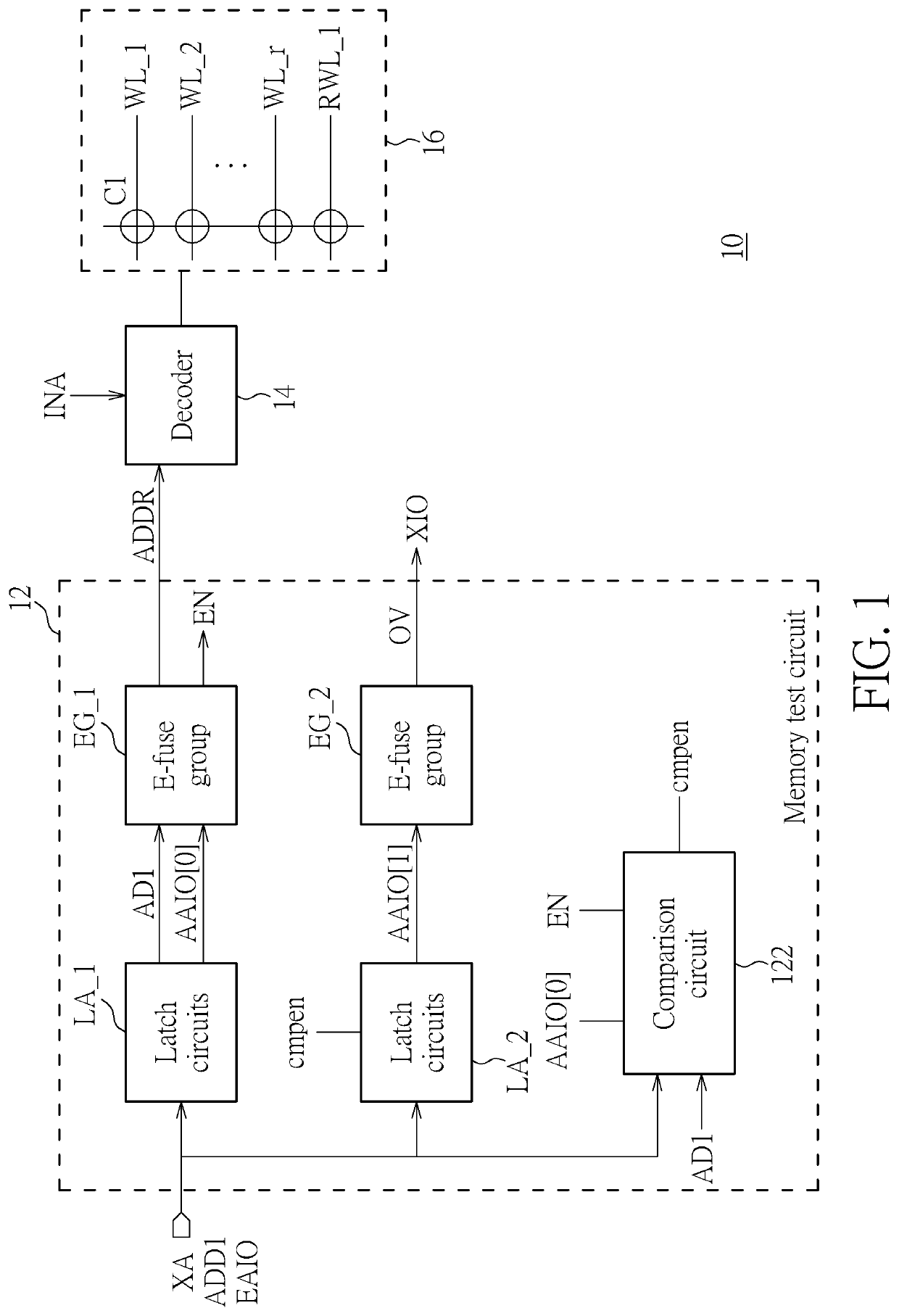
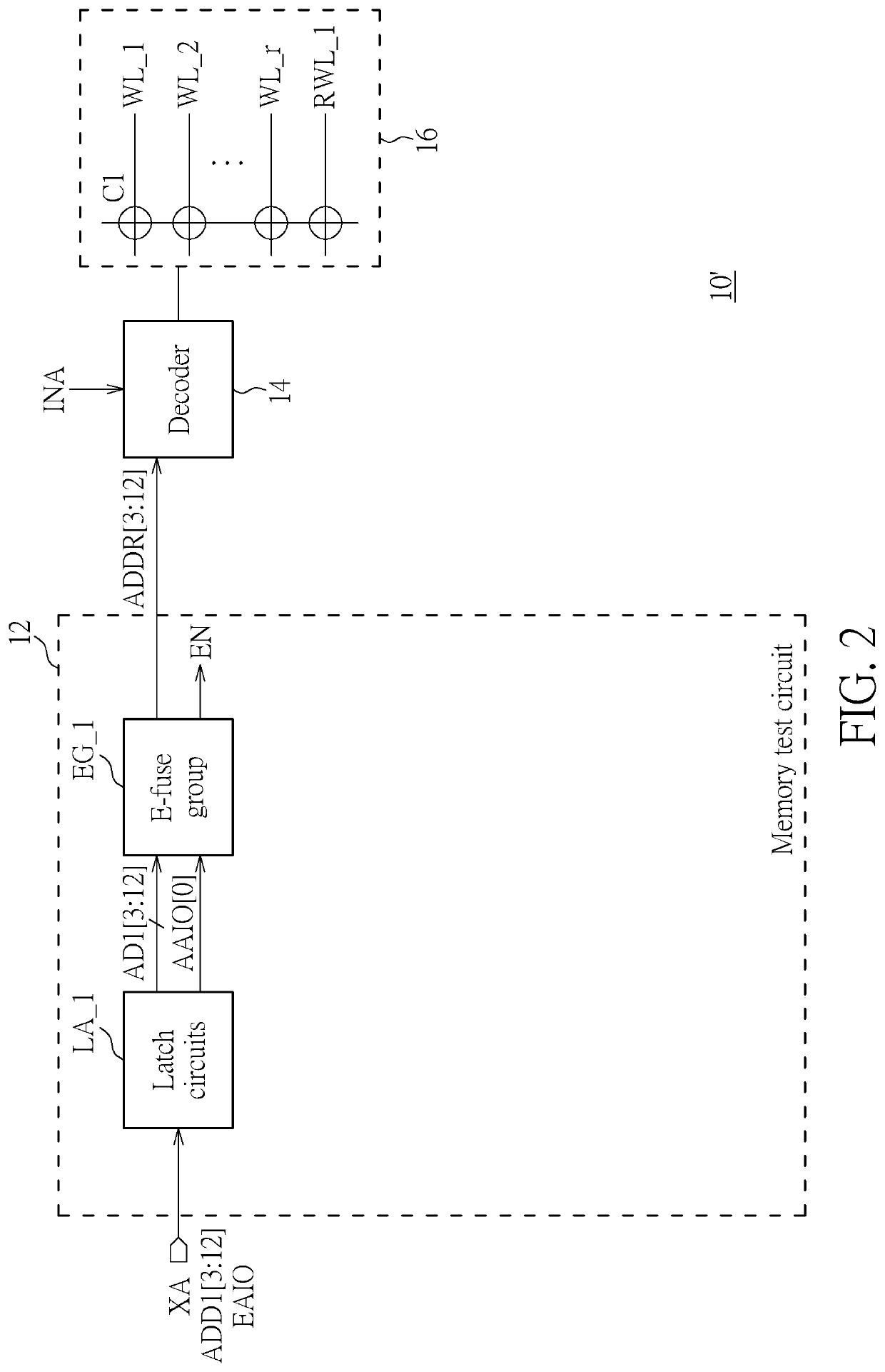
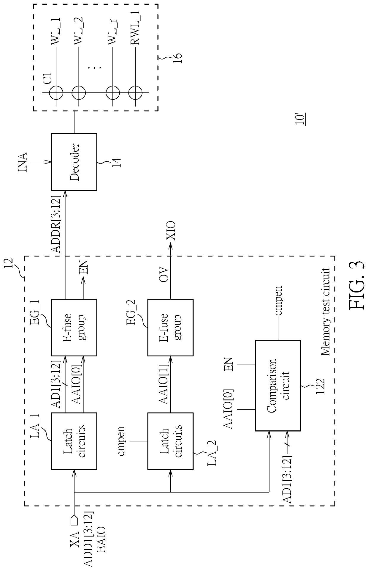
[0012]FIG. 1 is a block diagram illustrating a memory test circuit according to one embodiment of the present invention. The detailed operations will be illustrated below. Moreover, the memory test circuit described in the following embodiments is used in the FT mode, but the memory test circuit provid...


PUM


Abstract

A memory test circuit comprising: a first latch circuit for receiving a first input address and an error indication signal to generate a first address; a first E-fuse group for receiving the first address to generate an output address; a second latch circuit for receiving the error indication signal; a second E-fuse group for generating an error indication signal according to an output of the second latch circuit which is generated according to the fault indication signal; and a comparison circuit for activating the second latch circuit according to a relation between the first address and a second input address and a state of the first latch circuit or the first E-fuse group.

Description

BACKGROUND OF THE INVENTION1. Field of the Invention[0001]The present invention relates to a memory test circuit, and particularly relates to a memory test circuit which can automatically provide the error type of the memory device.2. Description of the Prior Art[0002]Memory test can usually be classified into chip probe (CP) test mode and final test (FT) mode. The CP test can also be called die test, and the final test is a test after the memory is packaged. The memory usually has multiple redundant word lines. When an error is found in the word line of the memory, the redundant word line is used to replace the word line with errors. However, in the FT mode, the memory can only store a very small number of addresses for word lines with errors, that is, only a very small number of redundant word lines can be used. When the number of addresses for word lines with errors is greater than the number of word line error addresses that can be stored, the memory will be determined as irrepa...

Claims


Application Information

Patent Timeline
IPC IPC(8): G11C29/38G06F3/06G11C8/06
CPCG11C29/38G06F3/0653G11C8/06G06F3/0673G06F3/0619G11C2029/1208G11C2029/1202G11C29/56008G11C2029/4402
Inventor LIN, YU-TAOYAO, TSE-HUACHEN, YI-FAN
Owner ELITE SEMICON MEMORY TECH INC
Why Eureka
Try Eureka