Pass gate input buffer for a mixed voltage environment

a mixed voltage environment and input buffer technology, applied in logic circuits, pulse techniques, reliability increasing modifications, etc., can solve the problems of voltage difference between peripheral supply voltage and processor supply voltage to further increase, transistors may become damaged or fail to operate properly,

Inactive Publication Date: 2000-02-29
INTEL CORP
View PDF4 Cites 44 Cited by
  • Summary
  • Abstract
  • Description
  • Claims
  • Application Information

AI Technical Summary

Problems solved by technology

This behavior may cause the voltage difference between the peripheral supply voltage and the processor supply voltage to further increase.
When this voltage difference is exceeded, the transistor may become damaged or fail to operate properly.

Method used


Image

  • Pass gate input buffer for a mixed voltage environment
  • Pass gate input buffer for a mixed voltage environment
  • Pass gate input buffer for a mixed voltage environment

Examples


embodiment

A Specific Embodiment

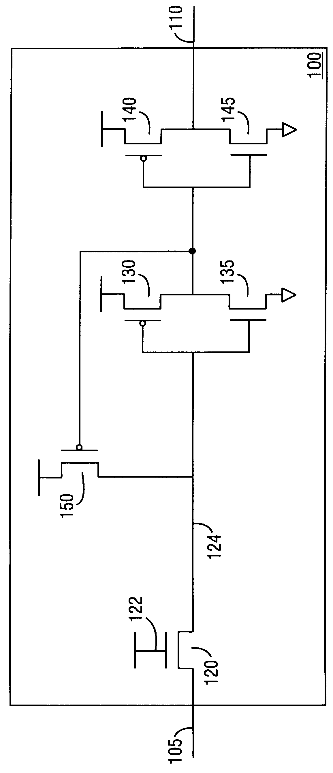
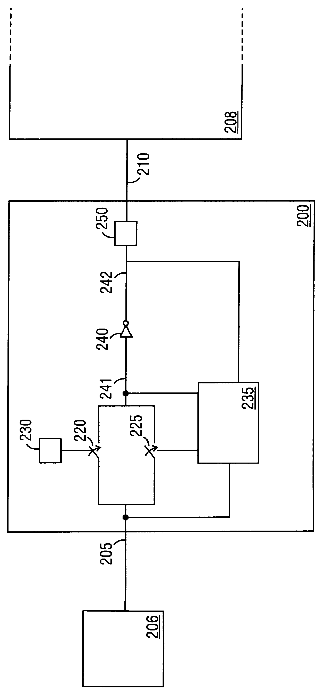
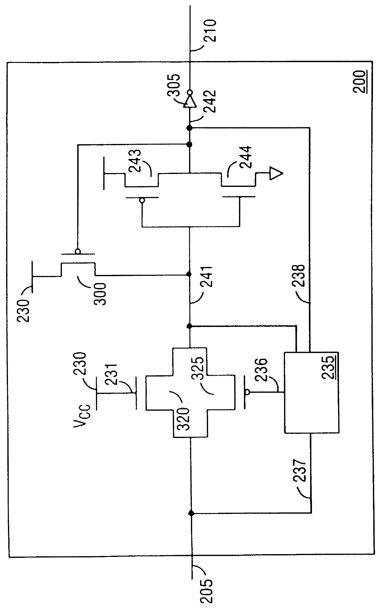
FIG. 3 is a schematic and block diagram of an embodiment of the input buffer 200, which is connected to at least one peripheral device by the line 205, and is connected to the core circuit 208 by the line 210. When a peripheral device applies a signal to the line 205, the signals are sent to the two pass gate transistors 320, 325. As previously mentioned, the transistors 320, 325 function essentially as switches in that they allow the voltage on the line 205 to be applied to the line 241 when they are active. The transistor 320 has an enable terminal coupled to a core reference voltage supply such that the voltage V.sub.cc is applied to the gate terminal 231 of the transistor 320. This causes the NMOS pass gate transistor 320 to remain active. One skilled in the art will appreciate that though the transistors 320, 325 are MOS (metal oxide semiconductor) transistors, they may be replaced by any transistor topology (e.g., bipolar transistors and field effect trans...


PUM


Abstract

An input buffer to interface among devices on a main circuit board is described. The input buffer includes a first transistor coupled between a first terminal and an input terminal of an inverter. The first transistor has an enable terminal adapted to be coupled to a first voltage supply. A second transistor that is coupled between the first terminal and the input terminal is also included. The input buffer further includes a control circuit to enable the second transistor. The control circuit is coupled to the first terminal, an enable terminal of the second transistor, the input terminal, and an output terminal of the inverter. A method for buffering signals among devices on a main circuit board comprises receiving a first signal in a first state from a first device. A first portion of the first signal is transmitted through a first transistor. A second portion of the first signal is transmitted through a second transistor. A second signal is generated by applying the first signal to the enable terminals of the third and fourth transistors. The second signal is then transmitted to a second device.

Description

1. Field of the InventionThe invention relates in general to the field of logic circuits, and, more particularly, to logic circuits used in computer systems. Specifically, the invention relates to an input buffer to interface between a central processing unit and other components on a main logic circuit board within a mixed voltage environment.2. Description of the Related ArtWith the growing complexity of modern computer systems and the availability of various types of peripheral devices on the main circuit board, designers are constantly seeking more efficient methods to improve the circuits that serve as interfaces between these peripheral devices and the central processing unit.Typically, a voltage V.sub.cc is associated with a processor voltage supply, while a voltage V.sub.ccp is associated with a peripheral voltage supply. The peripheral voltage Vccp is often larger than the processor supply voltage. The voltage differences between these two voltage levels often warrant an in...

Claims


Application Information

Patent Timeline
Patent Type & Authority Patents(United States)
IPC IPC(8): H03K19/003
CPCH03K19/00315
Inventor WAYNER, ZELIG
Owner INTEL CORP
Why Eureka
Try Eureka