Waveform correction circuit
a waveform correction and circuit technology, applied in the direction of pulse manipulation, pulse technique, pulse delivery at different times, etc., can solve the problems of signal irregularity or change in waveform duty ratio, change in duty ratio
- Summary
- Abstract
- Description
- Claims
- Application Information
AI Technical Summary
Problems solved by technology
Method used
Image

Examples
first embodiment
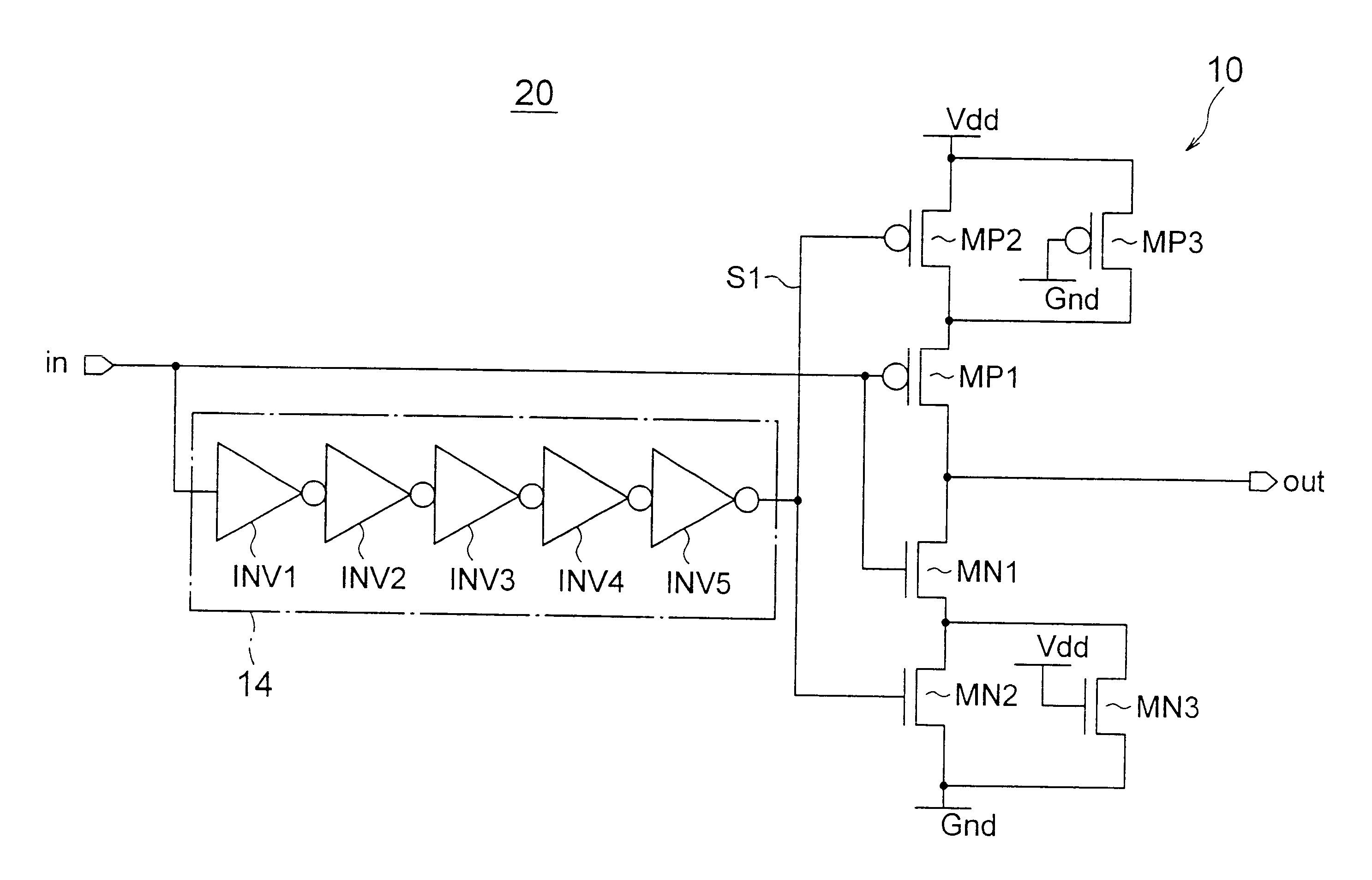
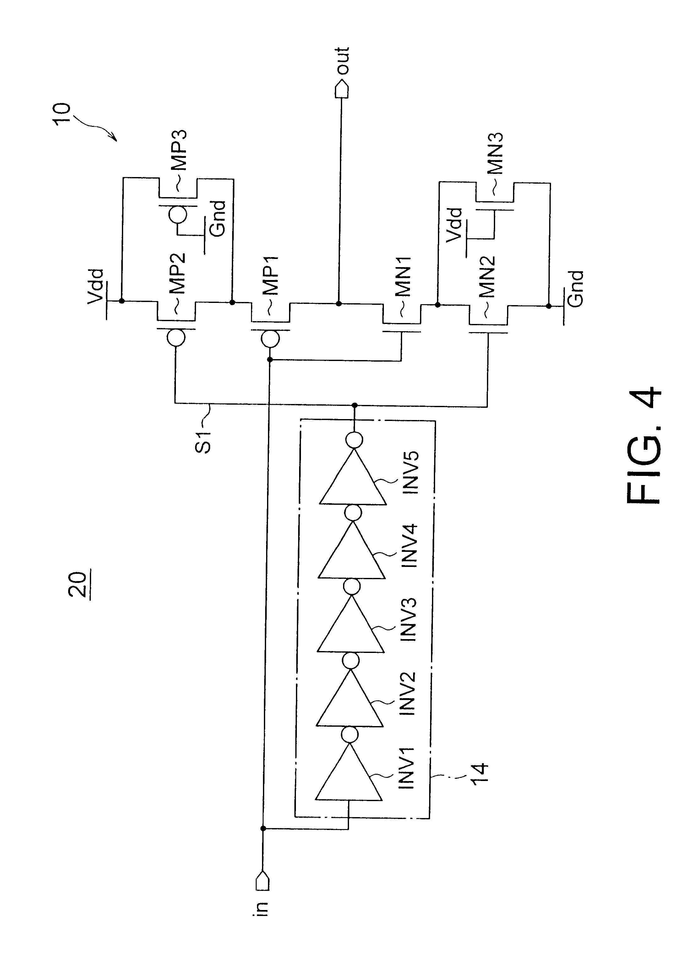
Referring to FIG. 4, a waveform correction circuit, generally designated by numeral 20, according to the present invention basically functions as an inverter. The waveform correction circuit or inverter circuit 20 includes a combination circuit 10 acting as an inverter, and a delay circuit 14 including an odd number of inverters INVL to INV5 and having an input connected to the input terminal. The combination circuit 10 includes a pMOSFET MP1, and an nMOSFET MN1 having a gate and a drain connected to the gate and the drain, respectively, of pMOSFET MP1. The gates of pMOSFET MP1 and nMOSFET MN1 constitute an input node or input terminal of the waveform correction circuit 20, whereas the drains of pMOSFET MP1 and nMOSFET MN1 constitute an output node or output terminal of the waveform correction circuit 20.
The combination circuit 10 further includes a pMOSFET MP2 connected between the source line Vdd and the source of pMOSFET MP1, an nMOSFET MN2 connected between the source of nMOSFET...
second embodiment
Referring to FIG. 5, a duty ratio correction circuit 40 according to the present invention includes first and second circuit blocks 15 and 16 each including a first inverter 22 or 21, a pair of waveform correction circuits 20-4, 20-1 or 20-3, 20-2, such as shown in FIG. 4, and a second inverter 23 or 24. The outputs of both the waveform circuits 20-4, 20-1 or 20-3, 20-2 are connected together to the input of the second inverter 23 or 24.
In the first circuit block 15, the first inverter 22 receives signal "A_" to deliver signal "B_", the waveform correction circuit 20-4 receives signal "B_" from the first inverter 22, the waveform correction circuit 20-1 receives signal "A", and the second inverter 23 receives synthesized signals from both the waveform correction circuits 20-4 and 20-1.
In the second circuit block 16, the first inverter 21 receives signal "A" to deliver signal "B", the waveform correction circuit 20-3 receives signal "B" from the first inverter 21, the waveform correc...
PUM
 Abstract
Description
Claims
Application Information
 - R&D Engineer
- R&D Manager
- IP Professional
- Industry Leading Data Capabilities
- Powerful AI technology
- Patent DNA Extraction
Browse by: Latest US Patents, China's latest patents, Technical Efficacy Thesaurus, Application Domain, Technology Topic.
© 2024 PatSnap. All rights reserved.Legal|Privacy policy|Modern Slavery Act Transparency Statement|Sitemap