Ink ejector that ejects ink in accordance with print instructions
- Summary
- Abstract
- Description
- Claims
- Application Information
AI Technical Summary
Benefits of technology
Problems solved by technology
Method used
Image
Examples
first embodiment
With reference to FIGS. 5A and 5B, an ink ejector 600 embodying the invention is mounted on a carriage (see reference numeral 3 in FIG. 7) for moving along a guide bar (not shown see reference numerals 7 and 8 in FIG. 7).
The ejector 600 includes a base wall 601 and a top wall 602, between which eight shear mode actuator walls 603a-603h extend. The actuator walls 603a-603h each consist of an upper part 605 and a lower part 607, which are made of piezo-electric material. The wall parts 605 and 607 are bonded to the top wall 602 and the base wall 601, respectively, and polarized in the opposite directions of arrows 609 and 611, respectively. The actuator walls 603a, 603c, 603e and 603g pair with the actuator walls 603b, 603d, 603f and 603h, respectively, to define a channel 613 between each pair of actuator walls. The actuator walls 603b, 603d and 603f pair with the actuator walls 603c, 603e and 603g, respectively, to define a space 615 between each pair of actuator walls. The three sp...
second embodiment
This embodiment explains a method of ejection control different from that described by the first embodiment. The ink ejectors for the two embodiments are substantially the same, but the signals for driving the actuators are different in waveform.
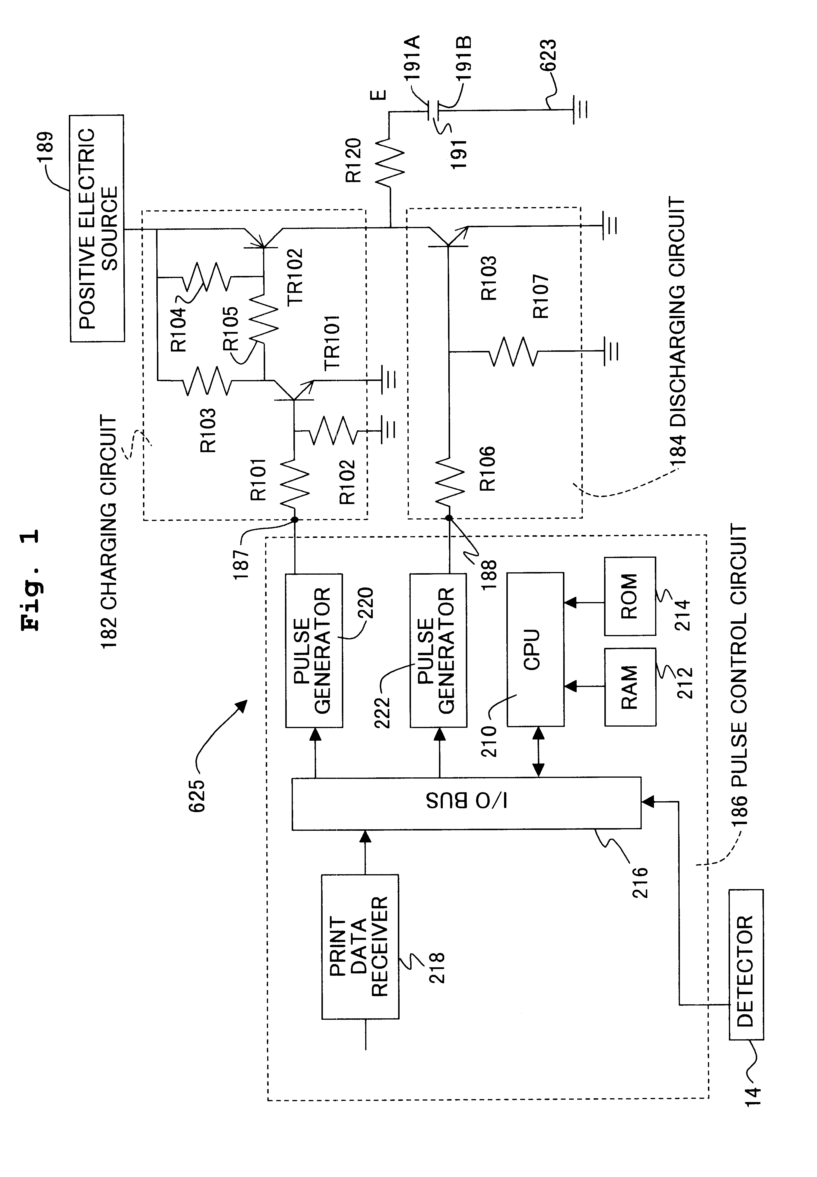
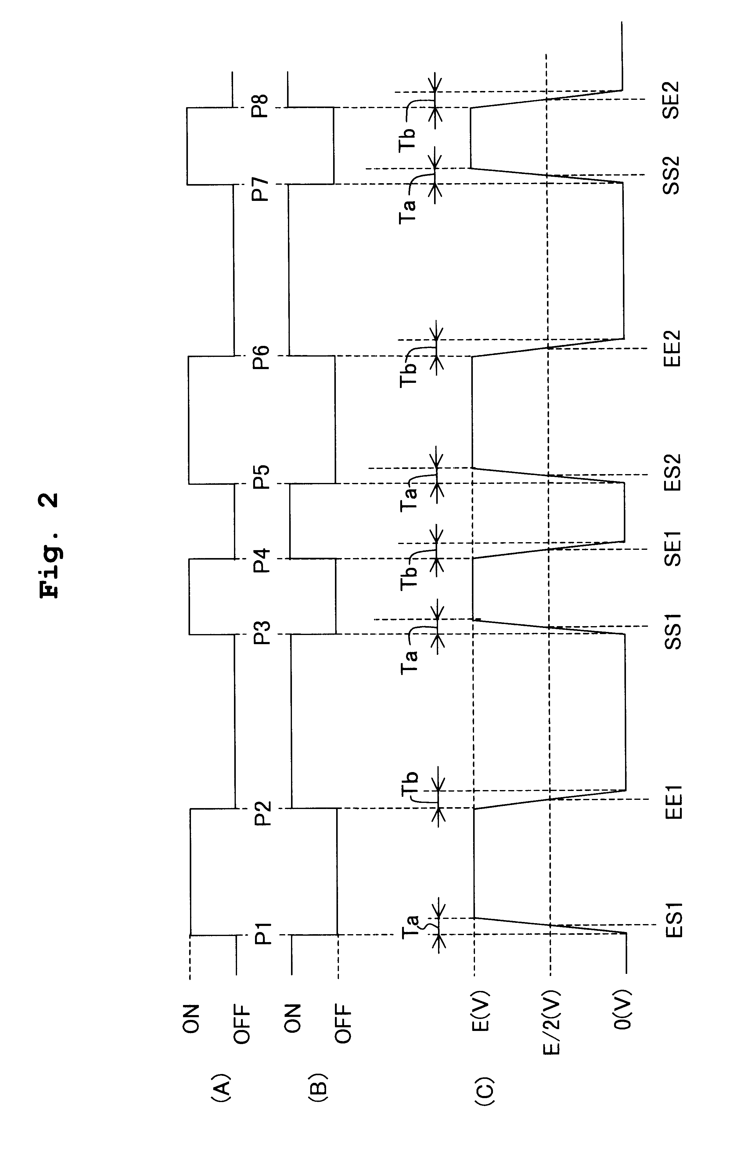
The signal input to the input terminal 187 of each charging circuit 182 shown in FIG. 1 is normally off, as shown in the timing chart of (A) in FIG. 8. For ejection of ink droplets, the input signal is rendered on at a point of time T1 and off at a point of time T2. Thereafter, the signal is alternately rendered on at points of time T (odd numbers) and off at points of time T (even numbers). When this signal is on (T1, T3 . . . , the signal input to the input terminal 188 of the associated discharging circuit 184 is rendered off, as shown in the timing chart of (B) of FIG. 8. When the signal input to the input terminal 187 of the charging circuit 182 is off (T2, T4 . . . ), the signal input to the input terminal 188 of the discharging circui...
PUM
 Abstract
Description
Claims
Application Information


