Method for supply voltage drop analysis during placement phase of chip design

a technology of supply voltage drop and placement phase, applied in the field of integrated circuit chips, can solve the problems of exacerbated noise problem, v.sub.dd supply voltage may not be available to power some circuits on the chip, and both approaches apply heuristic and expensive over-design

Inactive Publication Date: 2003-02-18
MARVELL ASIA PTE LTD
View PDF34 Cites 63 Cited by
  • Summary
  • Abstract
  • Description
  • Claims
  • Application Information

AI Technical Summary

Problems solved by technology

This further exacerbates the noise problem because the high current levels create local and often sizable resistive voltage drops in the power supply wiring.
As a consequence, the full V.sub.dd supply voltage may not be available to power some of the circuits on the chip.
Both approaches apply heuristic and expensive over-design, often sacrificing performance, power consumption, chip area, and / or cost.
Moreover, problems related to noise sensitivity are commonly not detected until very late in the design cycle or, worse, after the chip has already been fabricated.
Subsequent solutions rely on expensive and time-consuming remodeling and simulation and / or redesign activity.
In practice, this has proven difficult--the quantities of placed circuit objects (tens of thousands or more) and the size of the full-chip power distribution are enormous.
Moreover, for realistic designs, it would not be unreasonable to require thousands of model updates and corresponding solutions before obtaining an acceptable result.

Method used


Image

  • Method for supply voltage drop analysis during placement phase of chip design
  • Method for supply voltage drop analysis during placement phase of chip design
  • Method for supply voltage drop analysis during placement phase of chip design

Examples


Embodiment Construction

)

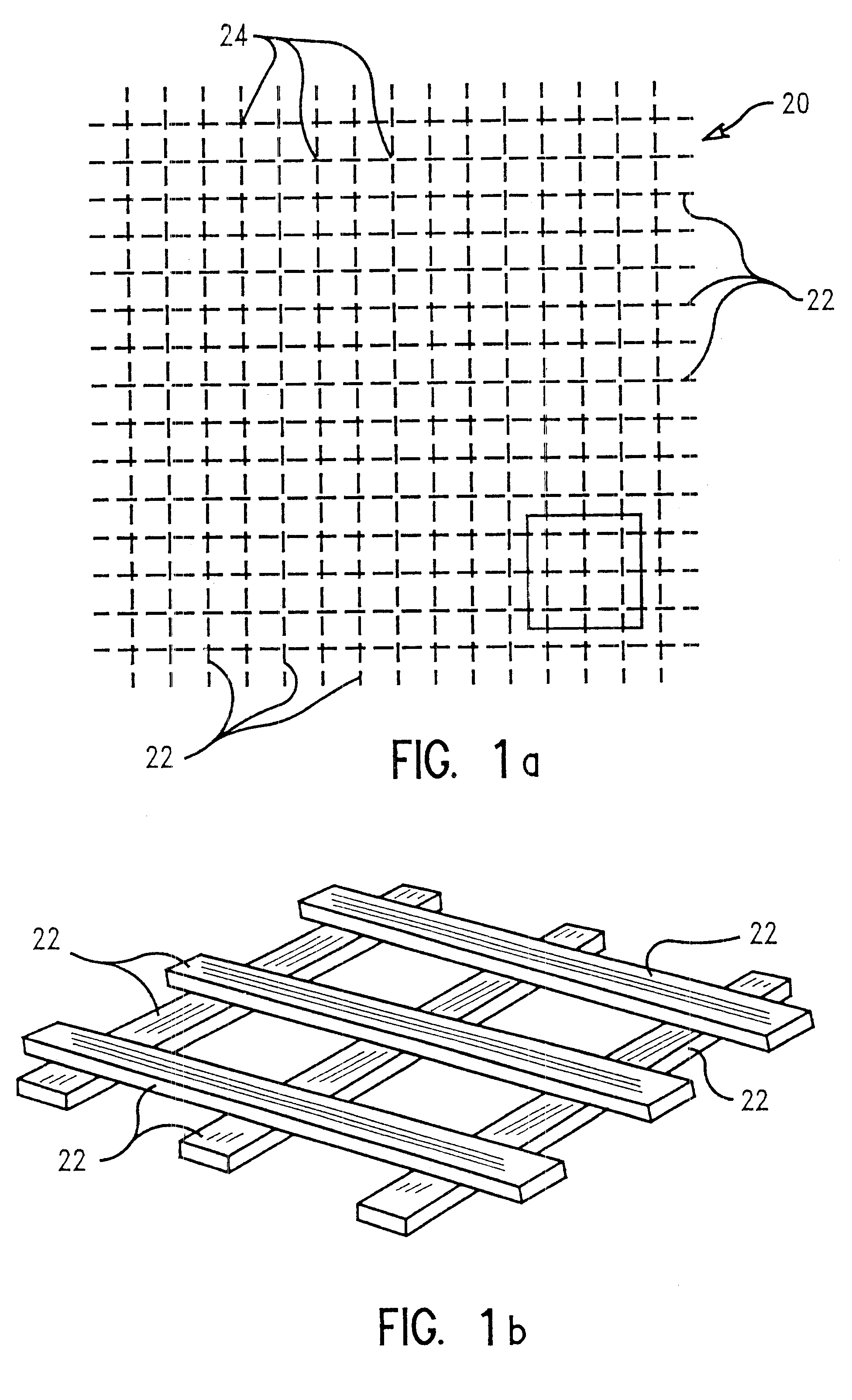
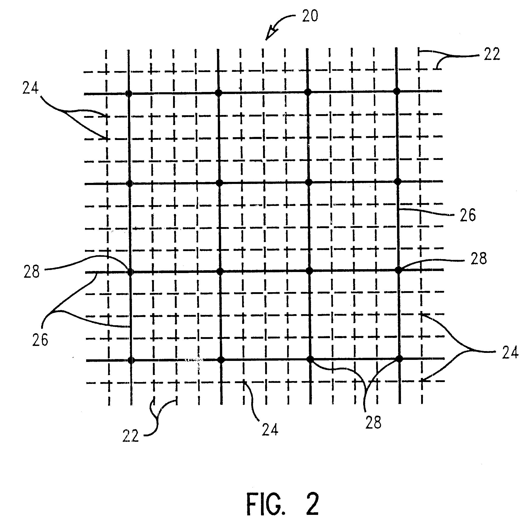
In describing the preferred embodiment of the present invention, reference will be made herein to FIGS. 1-8 of the drawings in which like numerals refer to like features of the invention. Features of the invention are not necessarily shown to scale in the drawings.

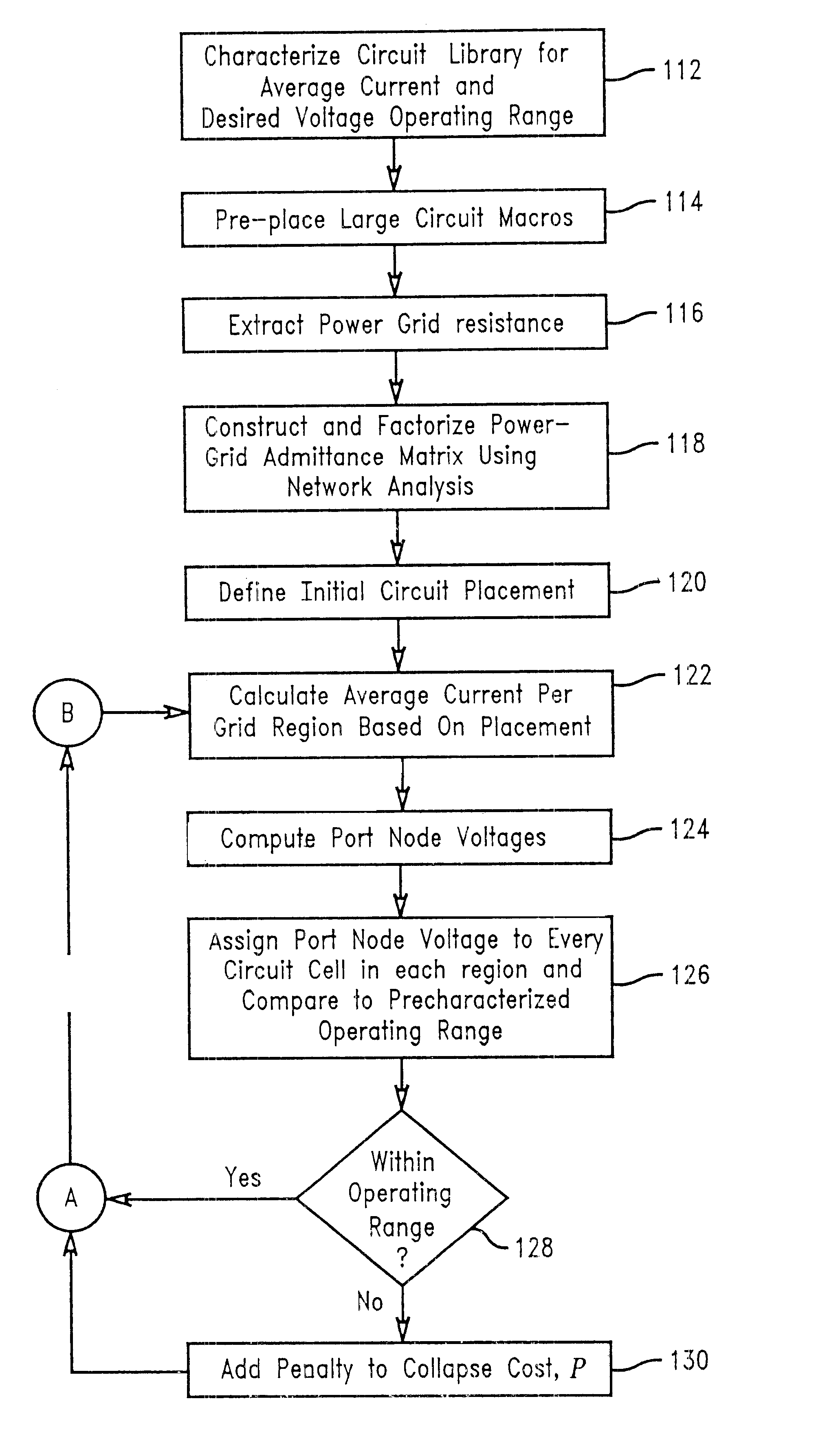
The present invention allows for the analysis of local and global voltage drop in the power grid of an integrated circuit during the floorplanning and circuit placement stage of chip design. A floorplanning / placement analysis tool has been employed in prior art circuit design methods, but without the consideration of circuit noise sensitivity, power supply voltage drop, and other features provided by the present invention, as will be described in detail below. Such analysis of local and global voltage drop in the power grid provides a means to assess potential power density or noise problems, whose early identification can facilitate the automatic generation of circuit layouts that are more immune to such problems. The pr...


PUM


Abstract

A method of analyzing supply voltage drops in a power grid for distributing power to an integrated circuit chip during design. The method initially comprises providing a library of circuits for use in designing an integrated circuit chip and determining a supply current requirement and an operating voltage range for each circuit in the circuit library. The method then includes calculating an admittance matrix representing the power grid with a pre-specified array of circuit ports defined by intersection of the power grid and a modeling grid, assigning regions of the power grid to each of the ports, and placing a set of circuits from the circuit library in regions on the power grid. The method further includes calculating a total node current at each of the ports by summing current requirements of all of the circuits located in the regions, calculating a node voltage at each of the ports by solving a system of linear equations corresponding to the calculated admittance matrix, imposing a penalty to each node having a node voltage outside of a predetermined range, and calculating the node voltages and the penalties to a cost-based floorplanning / placement analysis tool.

Description

1. Field of the InventionThe present invention relates to integrated circuit chips and, in particular, to power supply voltage analysis during the designing of such integrated circuit chips.2. Description of Related ArtA current technological trend in semiconductor design, especially for application specific integrated circuits (ASICs) and other advanced types of chips, is to reduce operating power. This trend drives the power supply voltages and, in turn, the device threshold voltages to lower levels. As the device threshold voltage V.sub.t and the power supply voltage V.sub.dd are reduced, the ratios of noise voltages to V.sub.t and V.sub.dd increase because the noise levels do not scale down at the same rate as V.sub.t and V.sub.dd. Consequently, circuit sensitivity to noise is increased.Modern technology trends also drive new designs to deliver higher levels of performance, most commonly achieved by increasing signal current levels and / or duty cycles. This further exacerbates th...

Claims


Application Information

Patent Timeline
Patent Type & Authority Patents(United States)
IPC IPC(8): G06F17/50
CPCG06F17/5072G06F17/5036G06F30/392G06F30/367
Inventor COHN, JOHN M.VENUTO, JAMESWEMPLE, IVAN L.ZUCHOWSKI, PAUL S.
Owner MARVELL ASIA PTE LTD
Why Eureka
Try Eureka