

Chip antenna
a chip antenna and antenna line technology, applied in the direction of helical antennas, non-resonant long antennas, protective materials radiating elements, etc., can solve the problem that the spiral pitch of the antenna line 130 cannot be reduced much
- Summary
- Abstract
- Description
- Claims
- Application Information
AI Technical Summary
Problems solved by technology
Method used
Image

Examples
first embodiment
, FIGS. 1 to 3
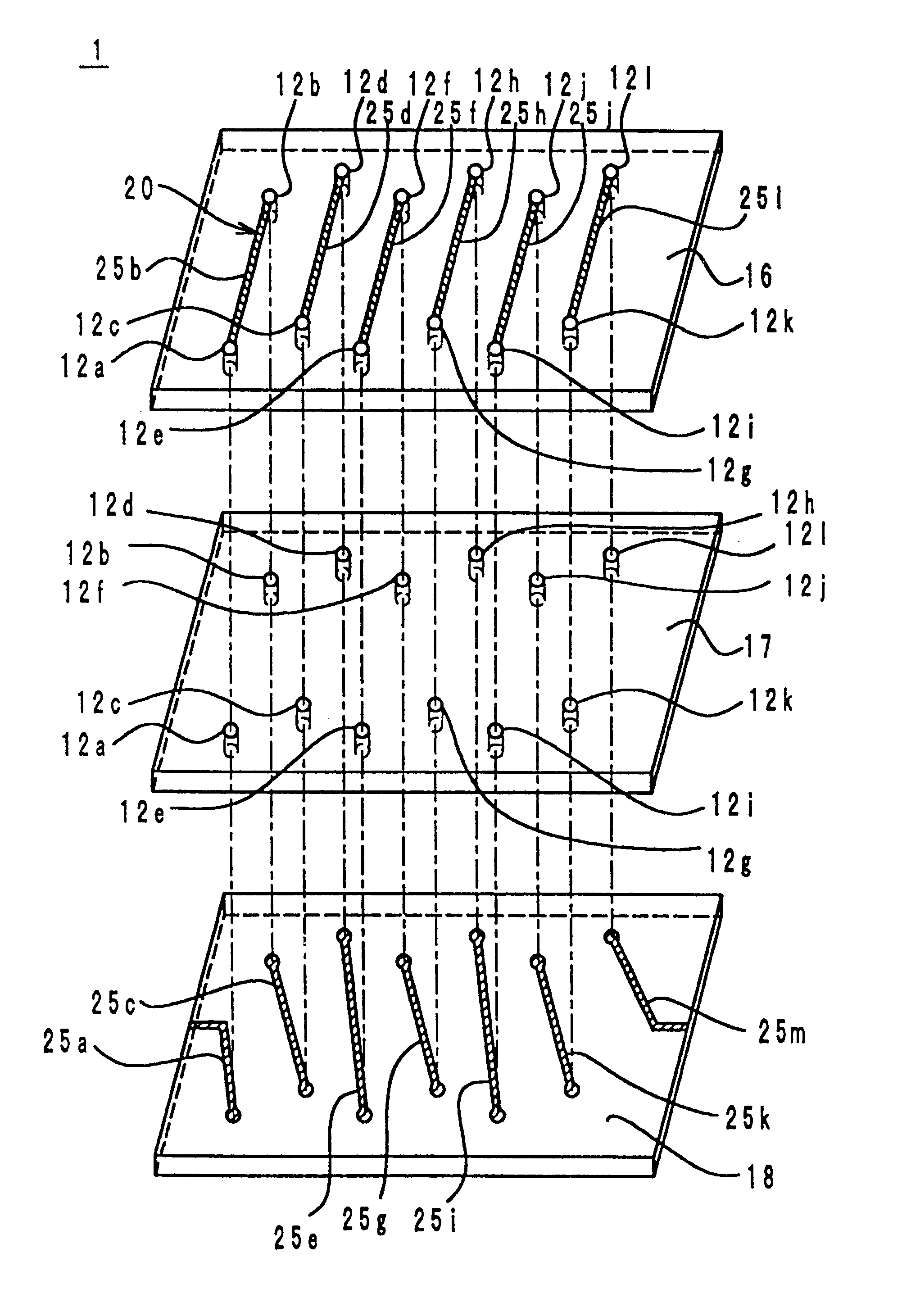
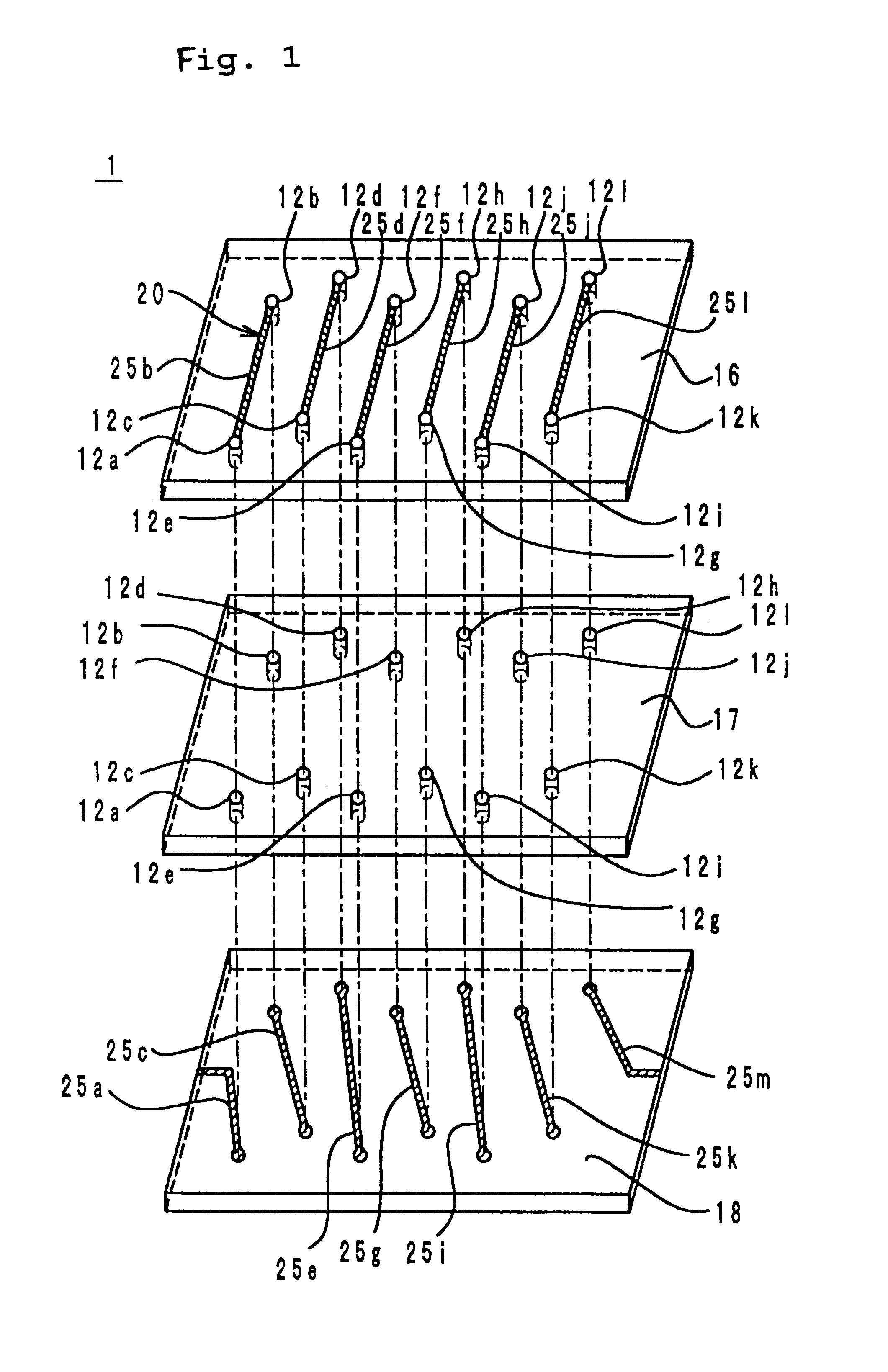
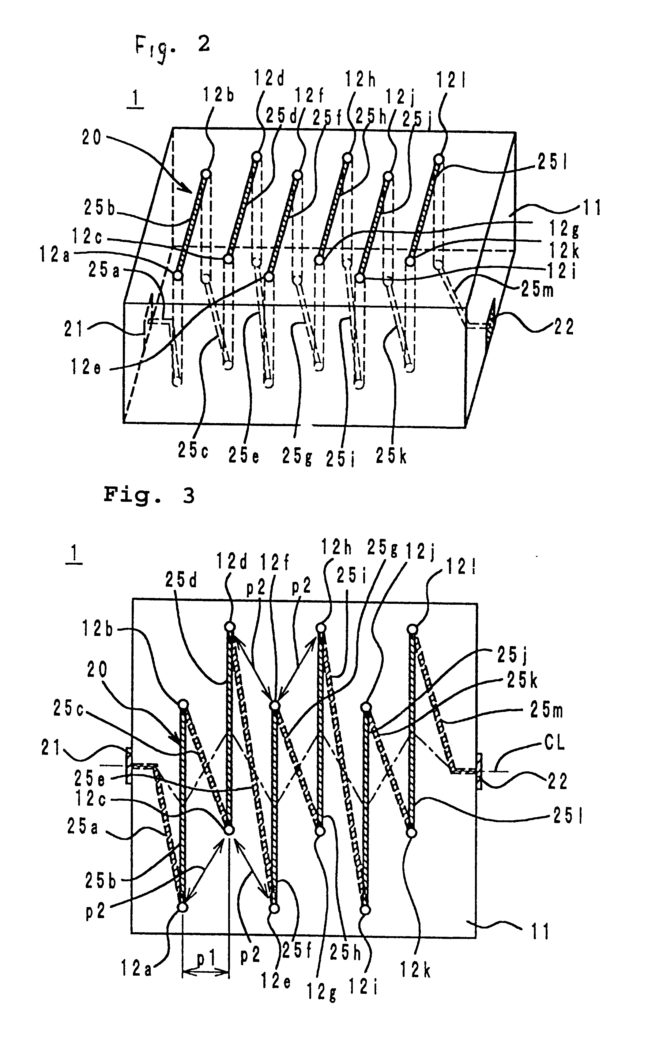
FIG. 1 is an assembly view showing a chip antenna 1; FIG. 2 is an external perspective view of the chip antenna 1 shown in FIG. 1; and FIG. 3 is a plan view of the chip antenna 1 shown in FIG. 1.
As is shown in FIG. 1, the chip antenna 1 comprises a dielectric sheet 16 having conductor patterns 25b, 25d, 25f, 25h, 25j, and 25l and via holes 12a to 121 formed thereon, a dielectric sheet 17 having the via holes 12a to 121 formed thereon, and a dielectric sheet 18 having conductor patterns 25a, 25c, 25e, 25g, 25i, 25k, and 25m formed on the top face of the dielectric sheet 18.
The conductor patterns 25a to 25m are formed on the surfaces of the respective dielectric sheets 16 and 18 by a method such as printing, sputtering, vapor deposition, pasting, or plating. As a material of the conductor patterns 25a to 25m, Ag, Ag--Pd, Au, Pt, Cu, Ni, etc., are used. As a material of the dielectric sheets 16 to 18, a resin such as a fluorocarbon resin, ceramic containing barium oxide, ...
second embodiment
, FIGS. 4 to 6
FIG. 4 is an assembly view of a chip antenna 2; FIG. 5 is an exterior perspective view of the chip antenna 2 shown in FIG. 4; FIG. 6 is a plan view of the chip antenna 2 shown in FIG. 4; however, in FIG. 6, an opposing conductor 23 for adjusting the resonance frequency and a via hole 32m are not shown.
As is shown in FIG. 4, the chip antenna 2 comprises a dielectric sheet 15 having the opposing conductor 23 for adjusting the resonance frequency and the via hole 32m formed thereon, a dielectric sheet 16 having conductor patterns 45b, 45d, 45f, 45h, 45j, and 45l and via holes 32a to 32l formed thereon, a dielectric sheet 17 having the via holes 32a to 321 formed thereon, and a dielectric sheet 18 having conductor patterns 45a, 45c, 45e, 45g, 45i, 45k, and 45m formed on the top face of the dielectric sheet 18.
The conductor patterns 45a to 45m are electrically connected sequentially in series via the via holes 32a to 32l formed on the dielectric sheets 16 and 17 so as to fo...
third embodiment
, FIG. 7
FIG. 7 is a plan view of a chip antenna 3 according to a third embodiment. In the third embodiment, a spiral antenna line 60 is arranged in a dielectric base body 11b, in which the diameter of the spiral line 60 increases gradually as the winding proceeds.
Conductor patterns 65a to 65m formed in the dielectric base body 11b are electrically connected sequentially in series through via holes 52a to 52l formed in the dielectric base body 11b so as to form a spiral antenna line 60. The conductor patterns 65b, 65f, and 65j and the conductor patterns 65d, 65h, and 65l are arranged at intervals of a predetermined pitch and each length thereof increases gradually in order. The via holes 52b, 52d, 52f, 52h, 52j, and 52l are arranged in a staggered arrangement. The via holes 52a, 52c, 52e, 52g, 52i, and 52k are also arranged in a staggered arrangement.
In the chip antenna 3 formed as described above, just like in the second embodiment, the antenna line 60 has a straight winding axis CL...
PUM
 Abstract
Description
Claims
Application Information