
Method and apparatus for planarizing surfaces of semiconductor device conductive layers

a semiconductor device and conductive layer technology, applied in the direction of electrical equipment, semiconductor/solid-state device manufacturing, basic electric elements, etc., can solve the problems of uneven removal rate of polishing materials, varying polishing time, and reducing the area available for surface wiring

Inactive Publication Date: 2003-07-15
GLOBALFOUNDRIES US INC
View PDF5 Cites 7 Cited by
  • Summary
  • Abstract
  • Description
  • Claims
  • Application Information

AI Technical Summary

Problems solved by technology

Increasing chip density has placed more components on semiconductor wafer surfaces, which in turn, has decreased the area available for surface wiring.
The as-plated surface of the copper layer is irregular, resulting in uneven polishing material removal rates and thus varying polishing times between wafers.
These variations may lead to over-polishing in some areas and underpolishing in other areas.
Imprecise polishing operations can yield undesirable short circuits or open circuits, which may cause a semiconductor device to operate inconsistently, or not at all.

Method used


Image

  • Method and apparatus for planarizing surfaces of semiconductor device conductive layers
  • Method and apparatus for planarizing surfaces of semiconductor device conductive layers
  • Method and apparatus for planarizing surfaces of semiconductor device conductive layers

Examples


Embodiment Construction

Illustrative embodiments of the invention are described below. In the interest of clarity, not all features of an actual implementation are described in this specification. It will of course be appreciated that in the development of any such actual embodiment, numerous implementation-specific decisions must be made to achieve the developer's specific goals, such as compliance with system-related and business-related constraints, which will vary from one implementation to another. Moreover, it will be appreciated that such a development effort might be complex and time-consuming but would nevertheless be a routine undertaking for those of ordinary skill in the art having the benefit of this disclosure.

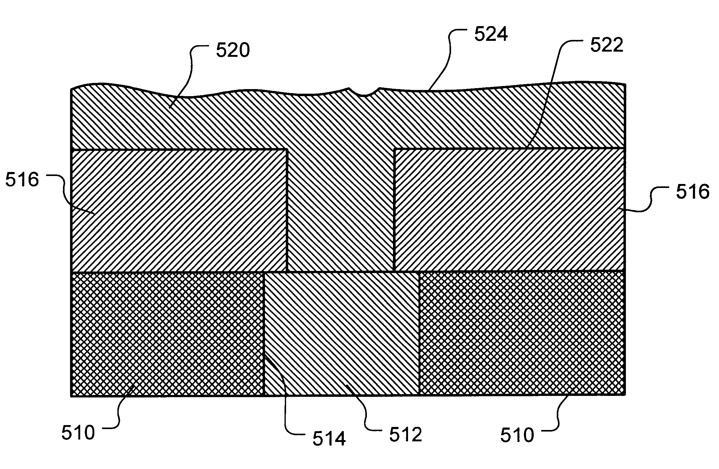
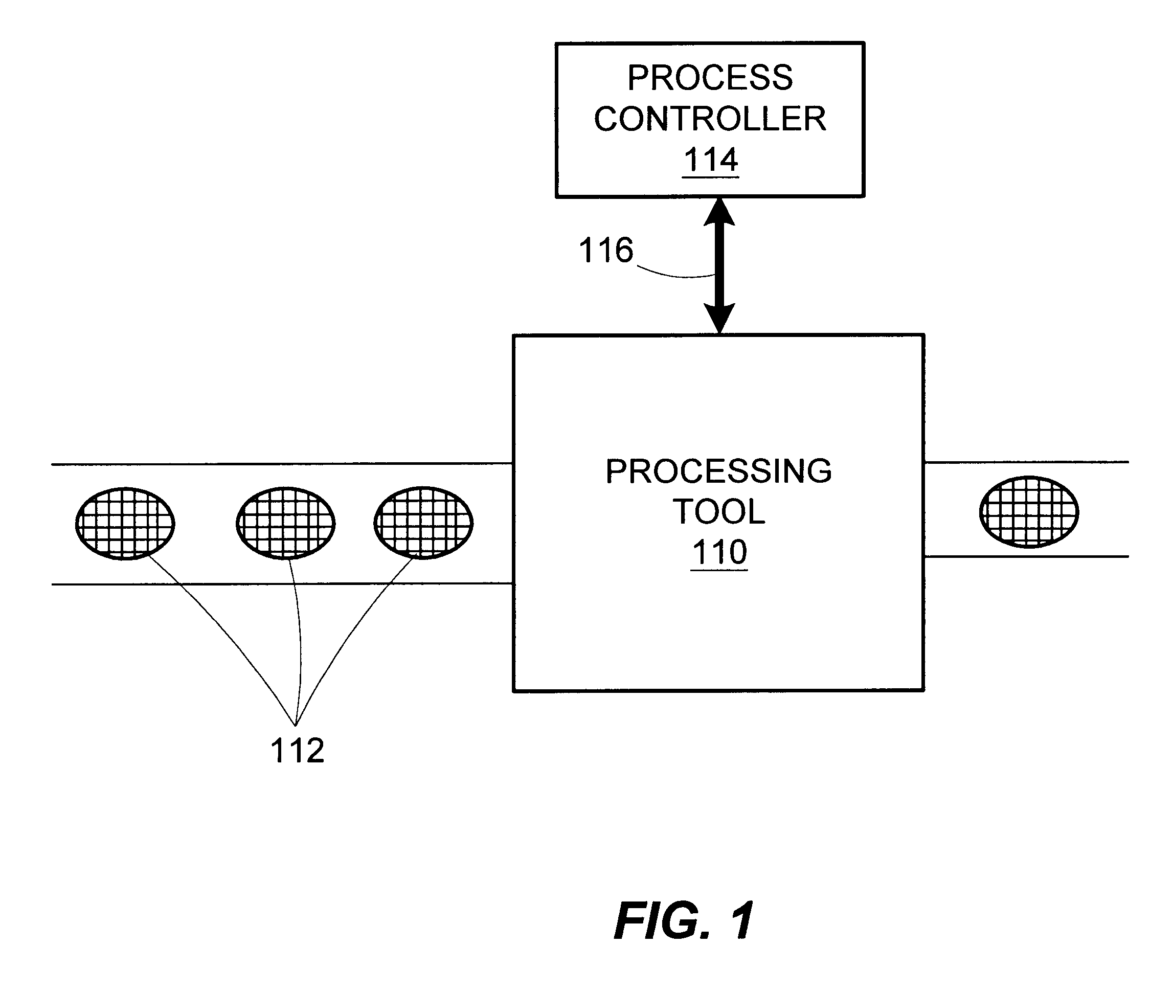
Referring to FIG. 1, an exemplary system according to the present invention including a processing tool 110 is shown. The processing tool 110 may be used as one part of an elaborate fabrication process to manufacture semiconductor wafers 112 into functional semiconductor devices. The pr...


PUM


Abstract

An apparatus and method are capable of a process to planarize a surface of a conductive layer on a semiconductor wafer. The method includes bringing a temperature of the conductive layer to within a predetermined range below a melting point of the conductive layer and holding the temperature of the conductive layer within the predetermined range to allow the conductive layer to undergo strain via at least one creep mechanism due to a weight of the conductive layer. The conductive layer is then cooled.

Description

1. Field of the InventionThe present invention relates to a method and apparatus for planarizing surfaces of semiconductor device conductive layers and, in one aspect, to a method and apparatus for planarizing such layers via creep strain.2. Description of the Related ArtIncreasing chip density has placed more components on semiconductor wafer surfaces, which in turn, has decreased the area available for surface wiring. The answer to this dilemma has been multilevel metallization schemes and an increased interest in copper conductors. As each layer of copper is deposited, typically via a plating process, the wafer is polished to remove excess copper and planarize the wafer layer. The as-plated surface of the copper layer is irregular, resulting in uneven polishing material removal rates and thus varying polishing times between wafers. Economics of semiconductor device manufacturing require that processes, such as those related to wafer polishing, be continually improved to decrease ...

Claims


Application Information

Patent Timeline
IPC IPC(8): H01L21/70H01L21/768
CPCH01L21/7684
Inventor RYSKOSKI, MATTHEW
Owner GLOBALFOUNDRIES US INC
Learn More