Method to produce a porous oxygen-silicon layer

a technology of oxygensilicon and oxygen, applied in the direction of semiconductor/solid-state device manufacturing, basic electric elements, electric devices, etc., can solve the problems of reducing the noise margin used, limiting the achievable speed, and complex methods described in the state of the ar

Inactive Publication Date: 2003-07-15
INTERUNIVERSITAIR MICRO ELECTRONICS CENT (IMEC VZW)
View PDF5 Cites 29 Cited by
  • Summary
  • Abstract
  • Description
  • Claims
  • Application Information

AI Technical Summary

Benefits of technology

The aim of the present invention is to increase the porosity of the CVD Silicon-oxygen film under soft physical and chemical conditions to avoid any change of the chemical composition and of the material properties. These physical and chemical conditions are compatible with the substrates and the layers formed thereon.
A key feature of the present invention is that the concentration of the HF in the ambient is determined such that the etching increases the pore size from 1 to 3 nm, without altering the thickness of the silicon-oxygen layer.

Problems solved by technology

This effect limits achievable speed and degrades the noise margin used to insure proper device operation.
The methods described in the state of the art are either complex or performed at very high temperatures (between 450 and 1200 degrees Celsius) and alters heavily the geometry of the silicon wafers and the integrated circuits formed on and in these silicon wafers or other substrates, liquefying most of the metals used in e.g. copper damascene back-end processing or e.g Aluminum-based metallisation schemes.
The problem to solve is the modification of the dielectric constant under soft physical and chemical conditions to preserve the geometry and the chemical composition of the porous insulating layer.

Method used


Image

  • Method to produce a porous oxygen-silicon layer
  • Method to produce a porous oxygen-silicon layer
  • Method to produce a porous oxygen-silicon layer

Examples


Embodiment Construction

The present invention discloses a way to prepare ultra low-k dielectric films with higher chemical stability compared to oxide and silsesquioxane-based porous materials.

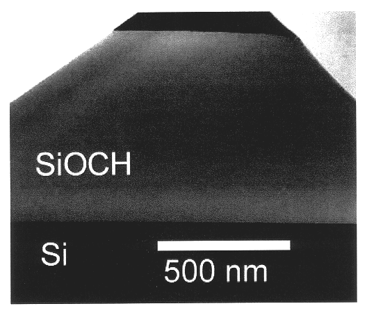
The SiOCH low-k films were deposited by a plasma enhanced oxidation of (CH.sub.3)SiH by N.sub.2 O at 400.degree. C. in the Applied Material P5000 chemical vapor deposition tool. The as-deposited SiOCH film had a dielectric constant close to 2.7 and a refractive index of 1.41-1.43.

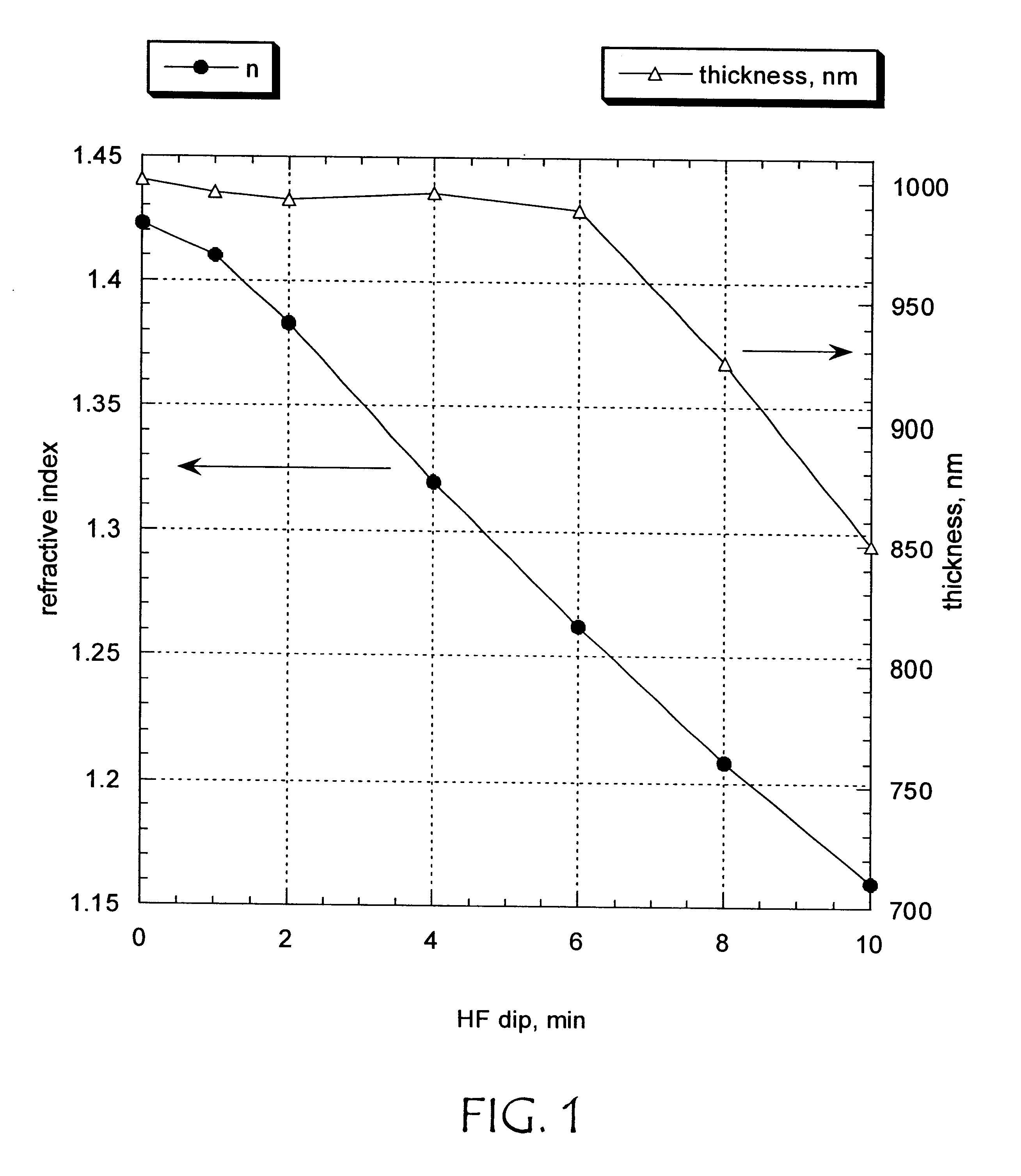
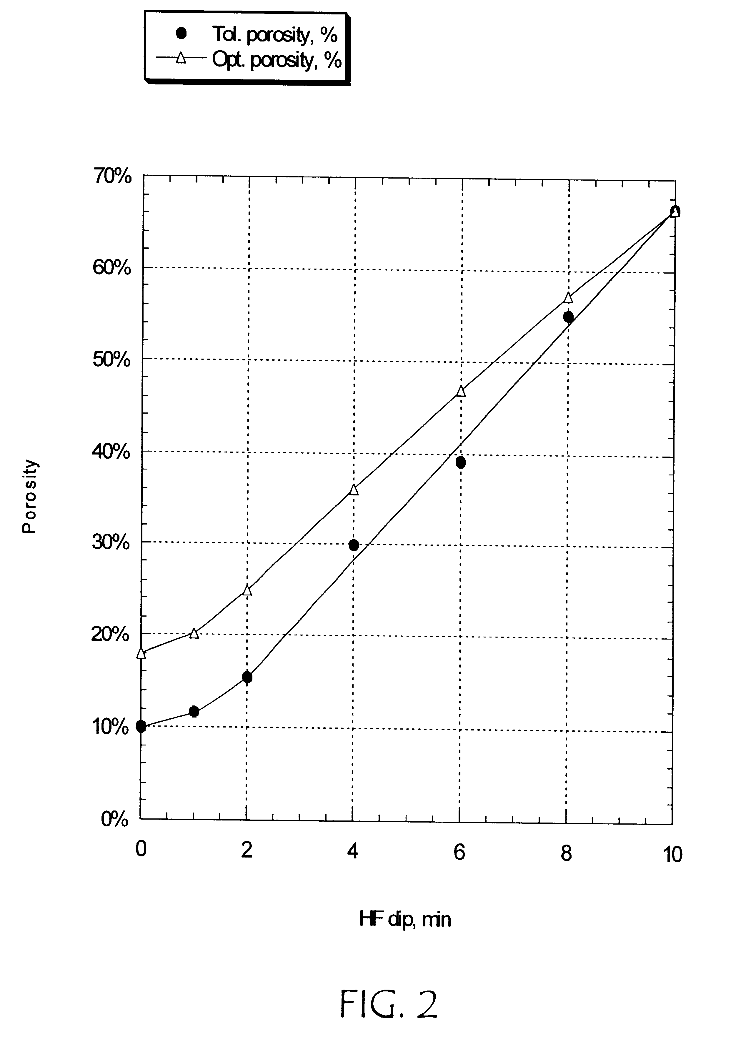
These films were etched in a diluted HF (2%) solution for various times (up to 10 minutes). Samples were etched at room temperature in a relatively large volume of solution (500 ml per 1 cm.sup.2 sample) and dried by compressed nitrogen.

After the etching, the refractive index and the thickness of the films were measured by ellipsometry (Sentech automatic single wavelength SE-401 ellipsometer).

The chemical composition of the SiOCH films was analyzed by FTIR and X-ray photoelectron spectroscopy (XPS). The FTIR spectra were recorded on a Bio-Ra...


PUM

PropertyMeasurementUnit
dielectric constantaaaaaaaaaa
thicknessaaaaaaaaaa

Abstract

The present invention concerns a method to produce a porous oxygen-silicon insulating layer comprising following steps:applying a silicon oxygen layer to a substrateexposing the said substrate to a HF ambient.

Description

The present invention is situated in the field of microelectronics and more precisely related to a method of forming a porous dielectric layer having a low dielectric constant for reducing capacity coupling on a semiconductor device.STATE OF THE ARTIntegrated circuits combine many transistors on a semiconductor, e.g. a single crystal silicon, chip to perform complex functions.The continuing scaling down of transistor size makes very important the delay caused by resistance capacitance coupling of the interconnecting wiring. This effect limits achievable speed and degrades the noise margin used to insure proper device operation.In order to decrease this parasitic capacitance, materials with a low dielectric constant (low k-materials) are continuously developed.The most common semiconductor dielectric is silicon dioxide which has a dielectric constant of about 4. Air has a dielectric constant of 1.0, which makes it obvious to increase the amount of air incorporated in the dielectric l...

Claims


Application Information

Patent Timeline
Patent Type & Authority Patents(United States)
IPC IPC(8): H01L21/02H01L21/312H01L21/316
CPCH01L21/02126H01L21/02203H01L21/02211H01L21/02274H01L21/02343H01L21/3121H01L21/31633H01L21/31695
Inventor BAKLANOV, MIKHAILSHAMIRYAN, DENISMAEX, KARENVANHAELEMEERSCH, SERGE
Owner INTERUNIVERSITAIR MICRO ELECTRONICS CENT (IMEC VZW)
Why Eureka
Try Eureka