Shared photodetector pixel image sensor

a technology of photodetector and image sensor, which is applied in the field of shared photodetector pixel image sensor, can solve the problem of only adding more pixels

Inactive Publication Date: 2005-01-04
APTINA IMAGING CORP
View PDF3 Cites 51 Cited by
  • Summary
  • Abstract
  • Description
  • Claims
  • Application Information

AI Technical Summary

Benefits of technology

Photodetectors often accounts for one of the largest real estate use on the pixel substrate. In an embodiment, a plurality of the photodetectors are associated with structure that allows the single photodetector to be used with several different pixels.

Problems solved by technology

However, more pixels can only be added by either increasing the size of the substrate on which the pixels are located, or by reducing the size of the pixels themselves.

Method used


Image

  • Shared photodetector pixel image sensor
  • Shared photodetector pixel image sensor
  • Shared photodetector pixel image sensor

Examples


Embodiment Construction

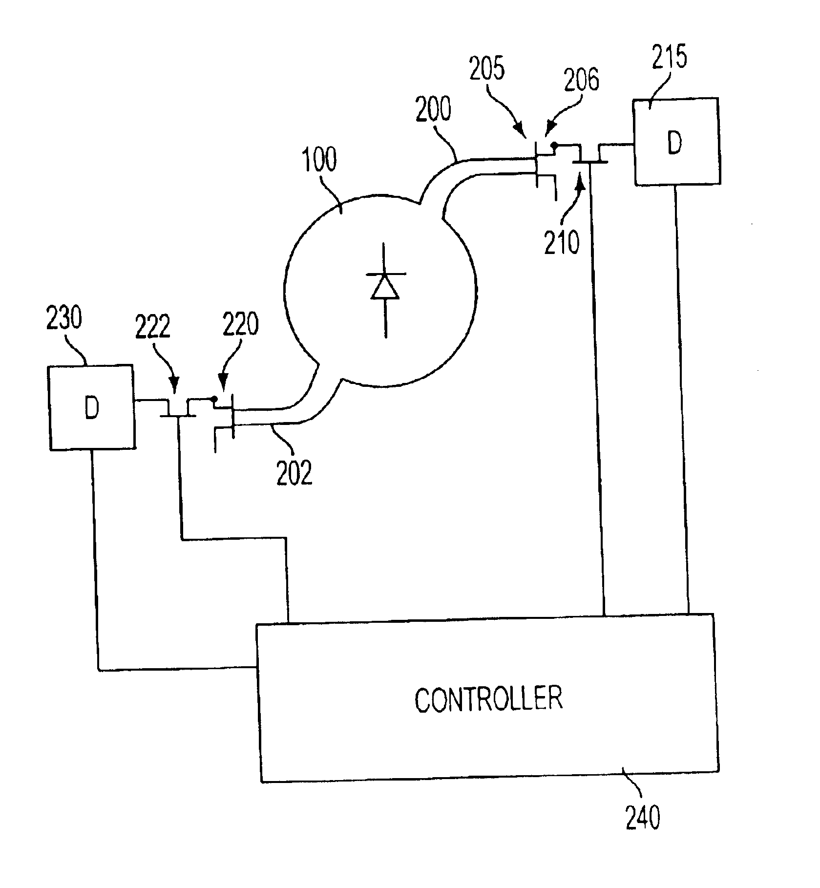
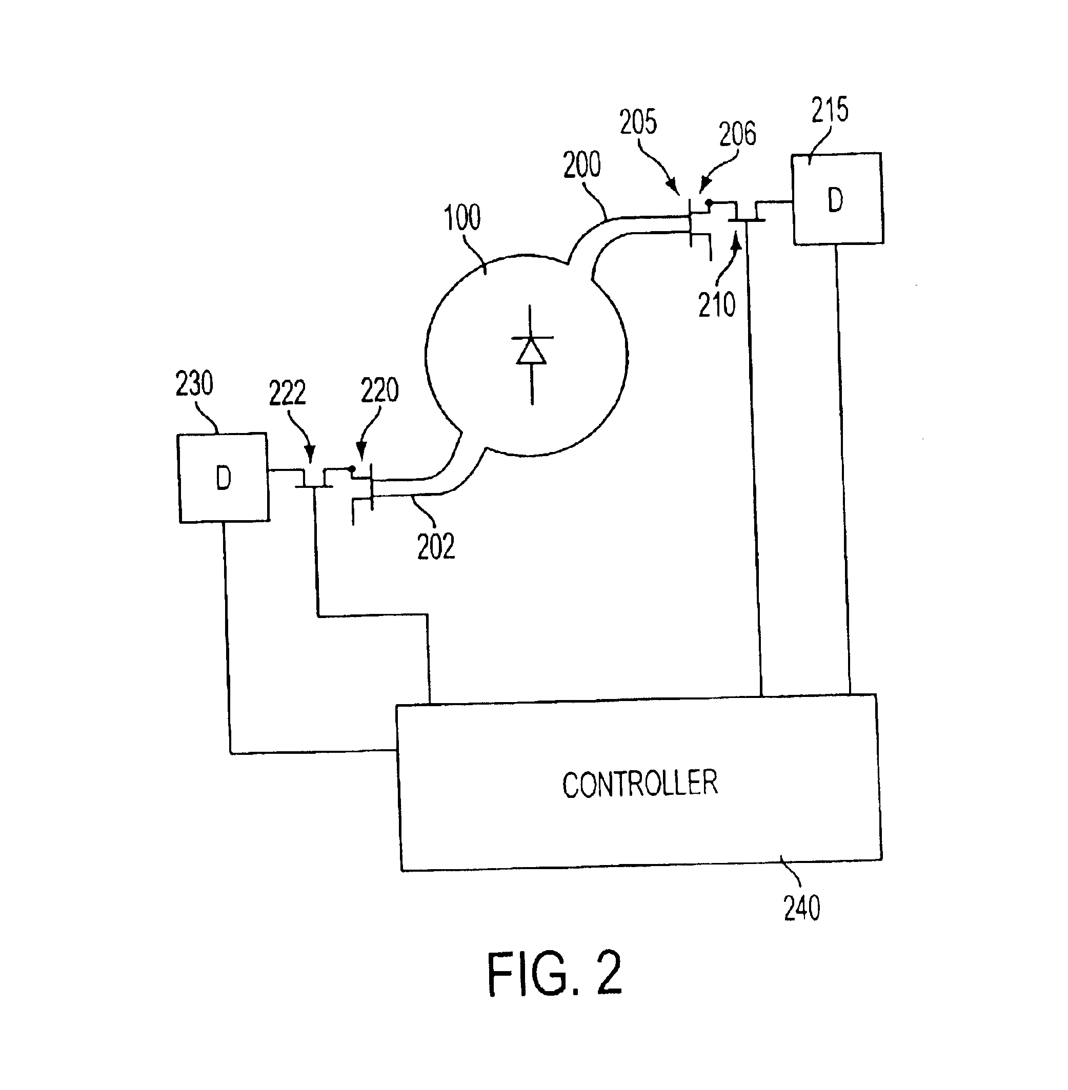
The present inventors recognized that the photodetector on an image sensor chip, such as an active pixel sensor, often takes up a large amount of area / real estate on the chip. In order to lower the fill factor in certain image sensors such as a freeze frame image sensor, the present system defines a device that shares a single photodetector among several pixels.

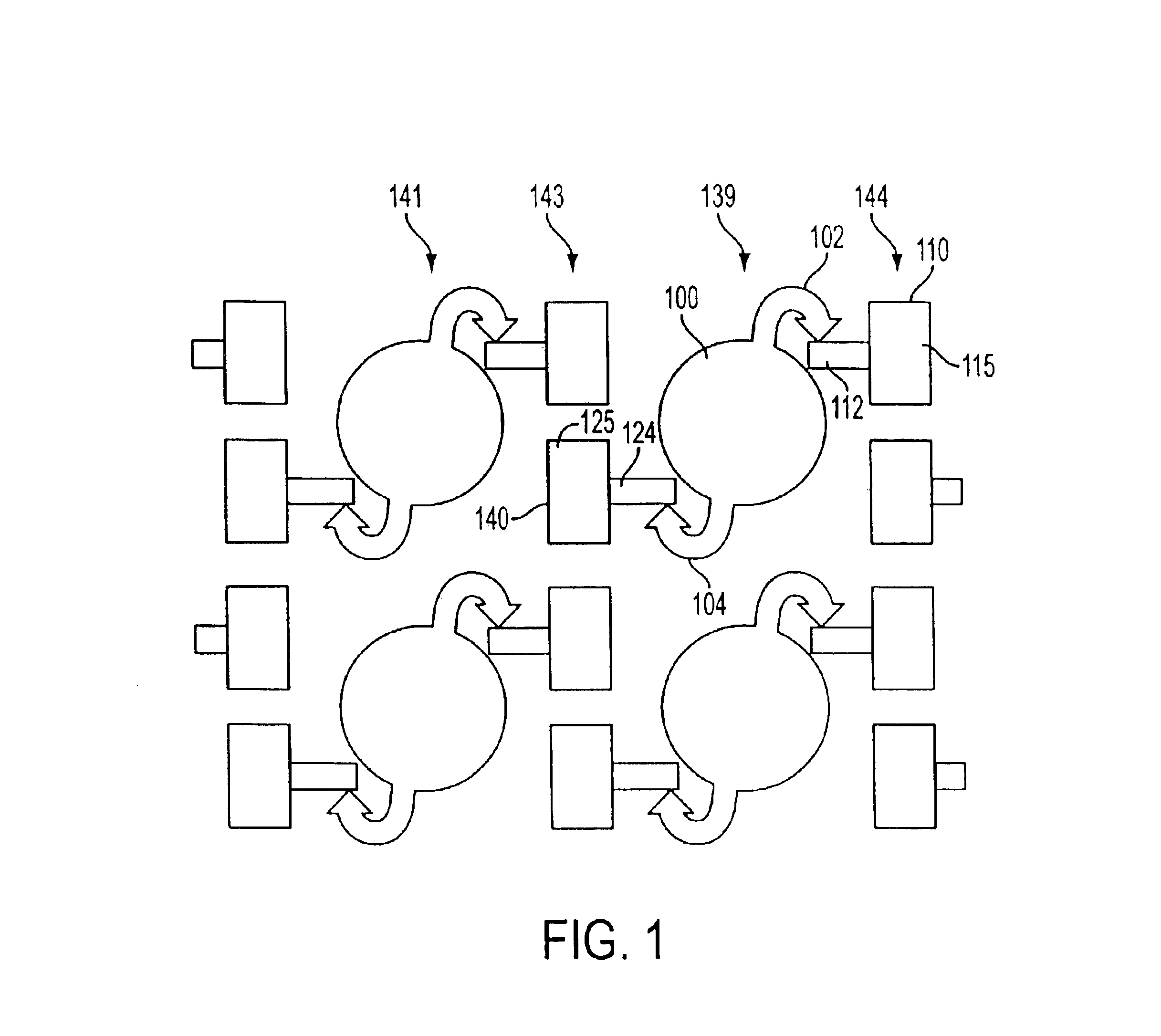
An embodiment is shown in FIG. 1. FIG. 1 shows four different photodetectors. Each photodetector such as 100 is shared between two different pixels.

At a first time, photodetector 100 accumulates signal representative of information for pixel 110. At a second time, photodetector accumulates signal for pixel 140. The photodetector 100 includes a first drain path 102 and a second drain path 104, both of which may always have the signal output thereon. A connection to the first drain path 102 provides the photodetector output to a first pixel 110. The connection includes a switch part 112 and a storage cell 115. The switch is act...


PUM


Abstract

A shared photodetector active pixel sensor uses a single photodetector between two different active pixels. The photodetector has a number of connection portions, which allow connecting to the different photodetector portions.

Description

BACKGROUND OF INVENTIONActive pixel sensors and other image sensors often have a trade-off between size of pixels in the sensor and the abilities of the sensor. More pixels may be more desirable, since it may enable the system to acquire light with a higher resolution. However, more pixels can only be added by either increasing the size of the substrate on which the pixels are located, or by reducing the size of the pixels themselves. In order to accommodate this trade-off, it may become important that the pixels be efficiently placed on the substrate. The fill factor refers to the way in which the pixels are placed on the substrate.Different pixel arrangements may have advantages in different situations. For example, active pixel sensors may be used for image acquisition, moving picture acquisition in either interlaced or non-interlaced format, and / or in freeze frame operations.SUMMARY OF INVENTIONThe present application teaches dual use of photodetectors on a substrate.Photodetect...

Claims


Application Information

Patent Timeline
Patent Type & Authority Patents(United States)
IPC IPC(8): H01L31/00H01L27/00H01L27/146
CPCH01L27/146
Inventor CAMPBELL, SCOTT PATRICKFOSSUM, ERIC R.
Owner APTINA IMAGING CORP
Why Eureka
Try Eureka