Reducing shunts in memories with phase-change material

a phase-change material and shunt technology, applied in the field of memories, can solve the problems of difficult determination of resistivity of phase-change material, poor adhesion between dielectric material and phase-change material,

Inactive Publication Date: 2005-03-01
MICRON TECH INC
View PDF1 Cites 332 Cited by
  • Summary
  • Abstract
  • Description
  • Claims
  • Application Information

AI Technical Summary

Problems solved by technology

One problem that arises is that the adhesion between the dielectric material and the phase-change material may be poor.
However, if that current is shunted past the phase-change material, the resistivity of the phase-change material may be harder to determine.

Method used


Image

  • Reducing shunts in memories with phase-change material
  • Reducing shunts in memories with phase-change material
  • Reducing shunts in memories with phase-change material

Examples


Embodiment Construction

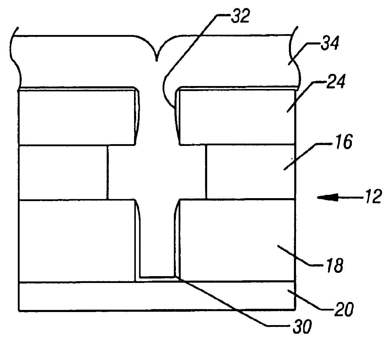
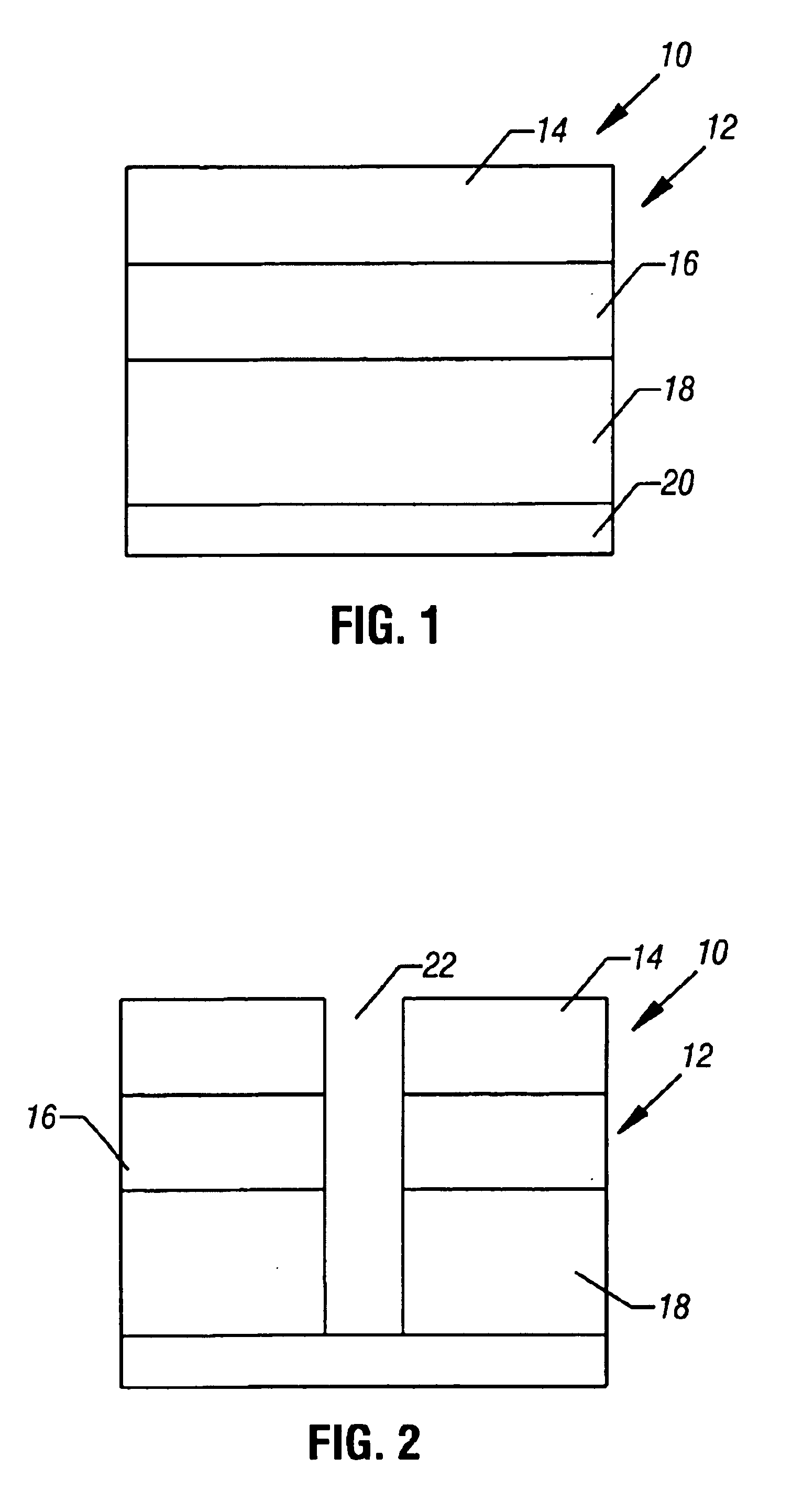
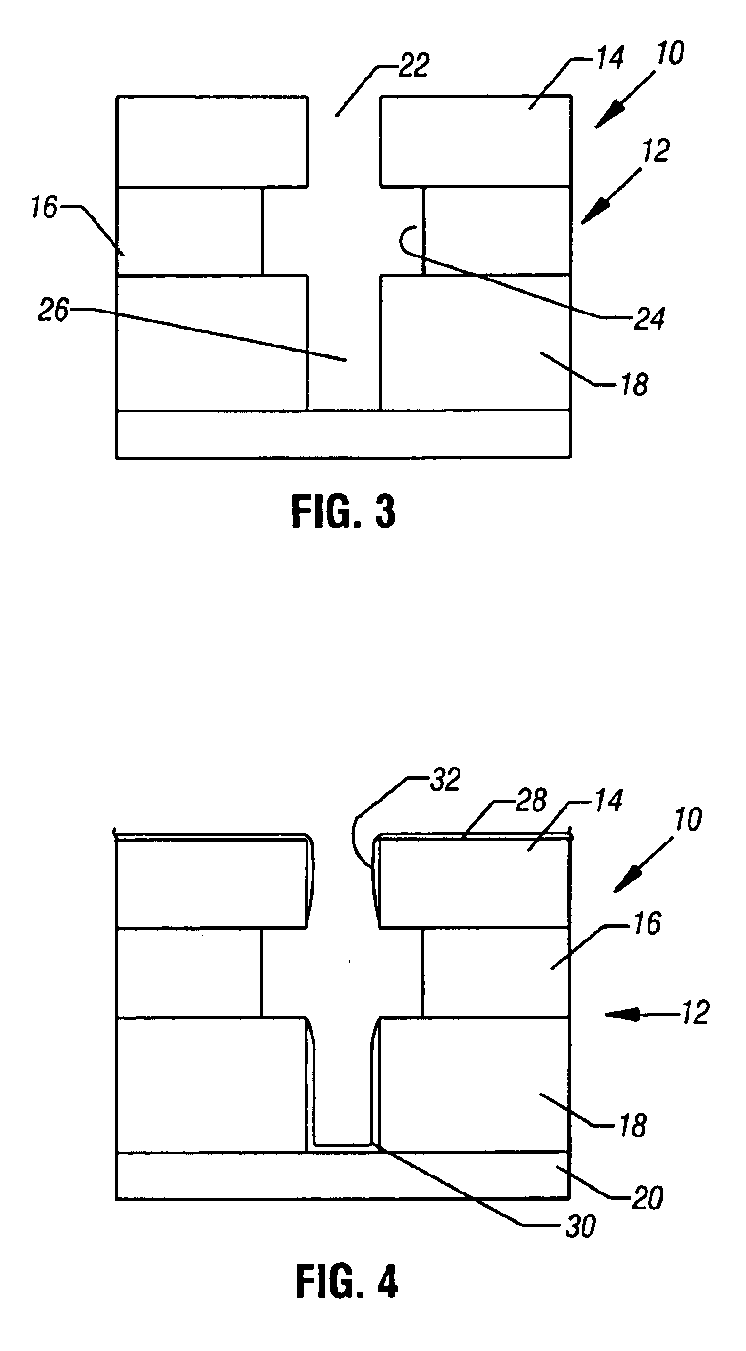
Referring to FIG. 1, a plurality of layers may be formed on a substrate or contact 20. The contact 20 may be cobalt silicide or any other conductive electrode in one embodiment. The contact 20 in some embodiments may be formed on still other structures. Over the contact 20 is a first dielectric layer 18. Over the first dielectric layer 18, may be a second dielectric layer 16. Over the second dielectric layer 16 may be a third dielectric layer 14 in one embodiment of the present invention. The dielectric layers 14, 16 and 18 define a dielectric 12, in accordance with one embodiment of the present invention, of a memory cell 10. In one embodiment, a nitride oxide nitride dielectric 12 may be utilized.

In accordance with one embodiment of the present invention, at least one layer of the dielectric 12 may be selectively and differentially etched. While an embodiment is shown with three layers, two or more layers may be utilized in other embodiments.

Referring to FIG. 2, in accordance with...


PUM


Abstract

A memory cell may include a phase-change material. Adhesion between the phase-change material and a dielectric or other substrate may be enhanced by using an adhesion enhancing interfacial layer. Conduction past the phase-change material through the interfacial layer may be reduced by providing a discontinuity or other feature that reduces or prevents conduction along said interfacial layer.

Description

BACKGROUNDThis invention relates generally to memories that use phase-change materials.Phase-change materials may exhibit at least two different states. The states may be called the amorphous and crystalline states. Transitions between these states may be selectively initiated. The states may be distinguished because the amorphous state generally exhibits higher resistivity than the crystalline state. The amorphous state involves a more disordered atomic structure and the crystalline state involves a more ordered atomic structure. Generally, any phase-change material may be utilized; however, in some embodiments, however, thin-film chalcogenide alloy materials may be particularly suitable.The phase-change may be induced reversibly. Therefore, the memory may change from the amorphous to the crystalline state and may revert back to the amorphous state thereafter or vice versa. In effect, each memory cell may be thought of as a programmable resistor, which reversibly changes between hi...

Claims


Application Information

Patent Timeline
Patent Type & Authority Patents(United States)
IPC IPC(8): H01L45/00
CPCH01L45/06H01L45/1683H01L45/144H01L45/1233H10N70/231H10N70/8828H10N70/826H10N70/066
Inventor XU, DANIELCHIANG, CHIEN
Owner MICRON TECH INC
Why Eureka
Try Eureka