Method and apparatus for translating detected wafer defect coordinates to reticle coordinates using CAD data

a technology of cad data and reticle coordinates, applied in the direction of semiconductor/solid-state device testing/measurement, image enhancement, instruments, etc., can solve the problems of only disposed defects, difficult and expensive to observe defects in wafers and reticles, and often only disposed defects

Inactive Publication Date: 2005-04-19
NXP USA INC
View PDF6 Cites 89 Cited by
  • Summary
  • Abstract
  • Description
  • Claims
  • Application Information

AI Technical Summary

Benefits of technology

[0009]According to another aspect of the invention, an apparatus includes a stage for holding a wafer under test, an image and defect detection device coupled to the stage for producing an inspection image of the wafer under test and for producing stage coordinates of defects detected in the wafer under test, CAD data for the wafer under test, a control...

Problems solved by technology

As geometries get smaller, the ability to observe defects in wafers and reticles (masks) becomes more challenging and expensive.
Existing wafer and reticle inspection tools...

Method used


Image

  • Method and apparatus for translating detected wafer defect coordinates to reticle coordinates using CAD data
  • Method and apparatus for translating detected wafer defect coordinates to reticle coordinates using CAD data
  • Method and apparatus for translating detected wafer defect coordinates to reticle coordinates using CAD data

Examples


Embodiment Construction

[0018]The invention and the various features and advantageous details thereof are explained more fully with reference to the nonlimiting embodiments that are illustrated in the accompanying drawings and detailed in the following description. It should be understood that the detailed description and the specific examples, while indicating specific embodiments of the invention, are given by way of illustration only and not by way of limitation. Various substitutions, modifications, additions and / or rearrangements within the spirit and / or scope of the underlying inventive concept will become apparent to those of ordinary skill in the art from this disclosure.

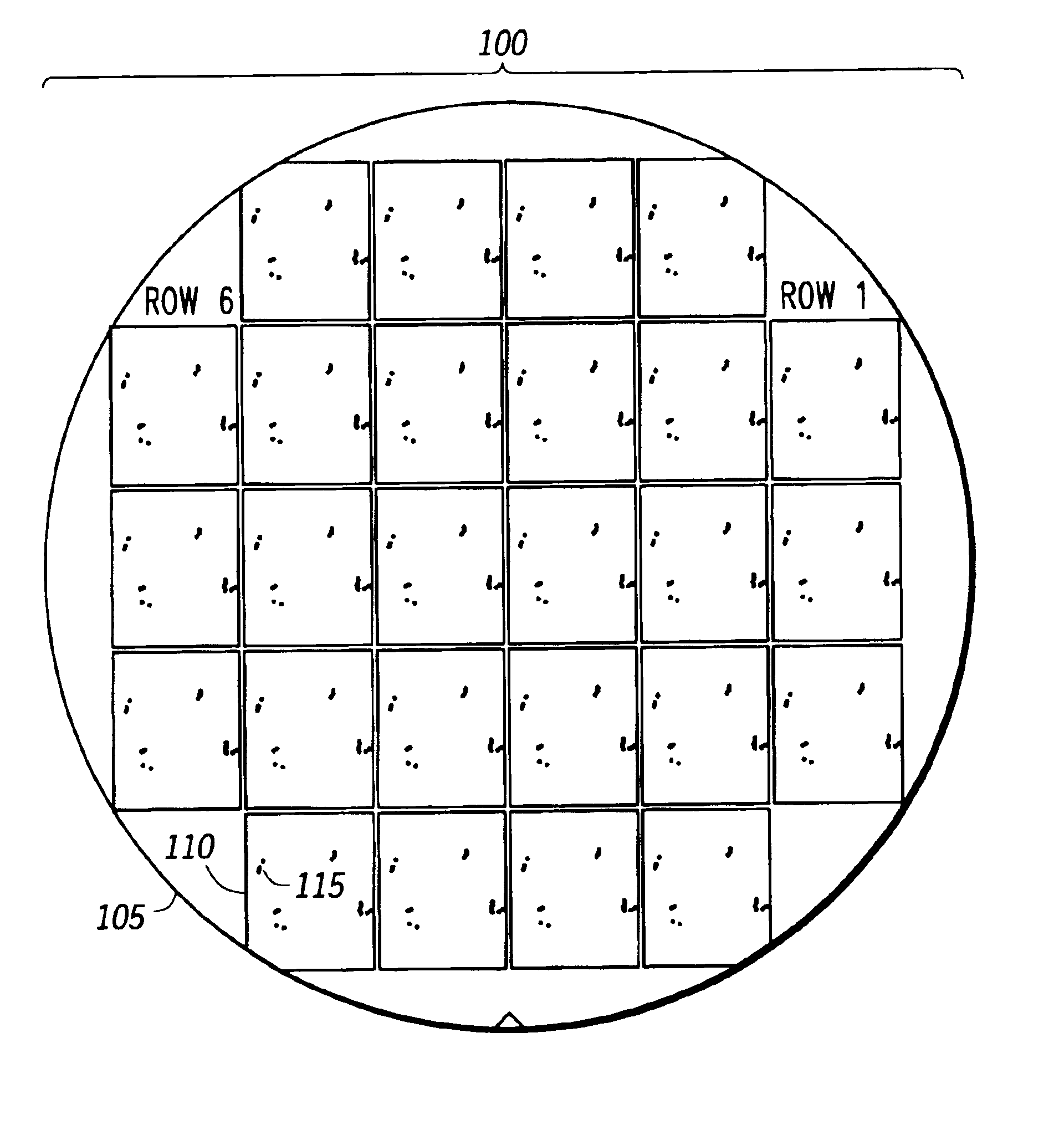
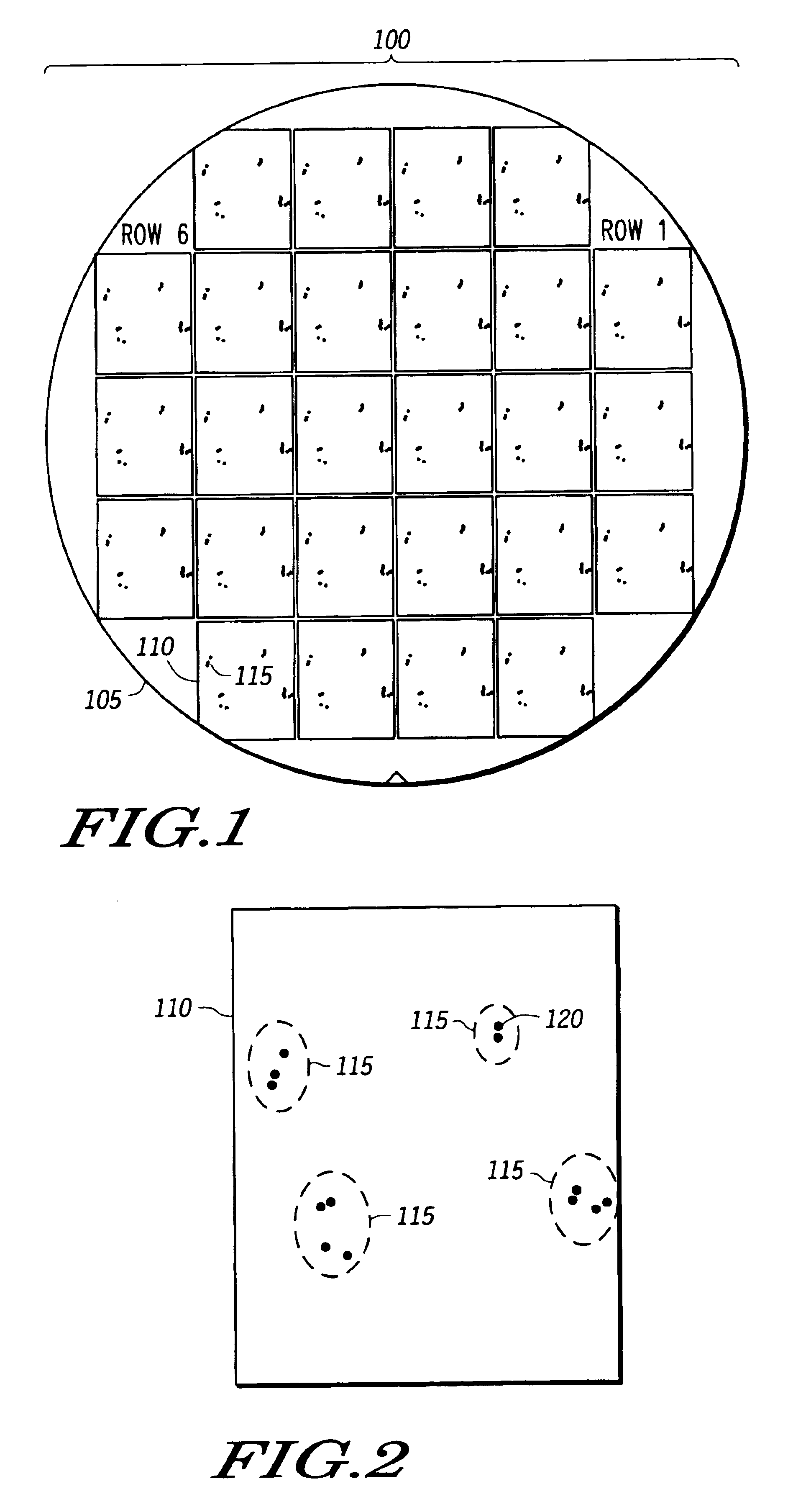
[0019]During inspection of wafers in a fabrication facility, repeater defects or anomalies may show up from time to time. Repeater defects are defects that are repeated in each reticle field of a wafer, and may be due to, for example, problems with the reticle mask or plate. When wafer defects are repeated from one reticle field to...


PUM


Abstract

Systems and methods are described for translating detected wafer defect coordinates to reticle coordinates using CAD data. A wafer inspection image is provided and coordinates of potential defects in the wafer are determined. Then the wafer inspection image is converted into a predetermined image format. CAD data for the device under test is then used to produce a second image, also in the predetermined image format. The CAD-derived image and the wafer-derived image are then aligned, and the coordinates of potential defects in the wafer are converted into CAD coordinates. The CAD coordinates are then used to navigate through the reticle for the wafer in order to locate reticle defects corresponding to the detected wafer defects.

Description

BACKGROUND OF THE INVENTION[0001]1. Field of the Invention[0002]The invention relates generally to the field of semiconductor manufacturing. More particularly, the invention relates to semiconductor inspection and measurement.[0003]2. Discussion of the Related Art[0004]Inspection and measurement are important areas of semiconductor manufacturing. Measurement may be defined as the ability to precisely quantify physical, dimensional, or electrical properties of different materials. Numerous measurement tools are routinely used to monitor the quality of semiconductor manufacturing processes. Inspection relates to the ability to observe and quantify defects, and inspection tools include a variety of optical instruments used for these purposes. In sub-micron applications, inspection equipment such as scanning electrical microscopes (SEMs) are widely used.[0005]As geometries get smaller, the ability to observe defects in wafers and reticles (masks) becomes more challenging and expensive. ...

Claims


Application Information

Patent Timeline
IPC IPC(8): G01N21/956G01N21/88G06T7/00G01Q90/00
CPCG01N21/95607G06T7/001G06T2207/30148H01L22/00
Inventor BRANKNER, KEITHSCHRAUB, DAVID M.
Owner NXP USA INC
Why Eureka
Try Eureka