
Plasma display panel and method of manufacturing partitions thereof

a technology of plasma display panel and manufacturing method, which is applied in the manufacture of electrode systems, electric discharge tubes/lamps, gas exhaustion means, etc., and can solve problems such as the complexity of structure of the panel

Inactive Publication Date: 2005-04-26
SAMSUNG SDI CO LTD
View PDF17 Cites 6 Cited by
  • Summary
  • Abstract
  • Description
  • Claims
  • Application Information

AI Technical Summary

Benefits of technology

[0012]To solve the above problem, it is an object of the present invention to provide a plasma display panel which can prevent a mis-discharge phenomenon in a non-light emitting zone.
[0013]It is another object of the present invention to provide a method of manufacturing partitions of the plasma display panel to prevent a mis-discharge phenomenon in the non-light emitting zone.

Problems solved by technology

However, since the above conventional technologies require an additional dummy electrode, the structures thereof become complicated.

Method used


Image

  • Plasma display panel and method of manufacturing partitions thereof
  • Plasma display panel and method of manufacturing partitions thereof
  • Plasma display panel and method of manufacturing partitions thereof

Examples


Embodiment Construction

[0036]Reference will now be made in detail to the present preferred embodiments of the present invention, examples of which are illustrated in the accompanying drawings, wherein like reference numerals refer to the like elements throughout. The embodiments are described below in order to explain the present invention by referring to the figures.

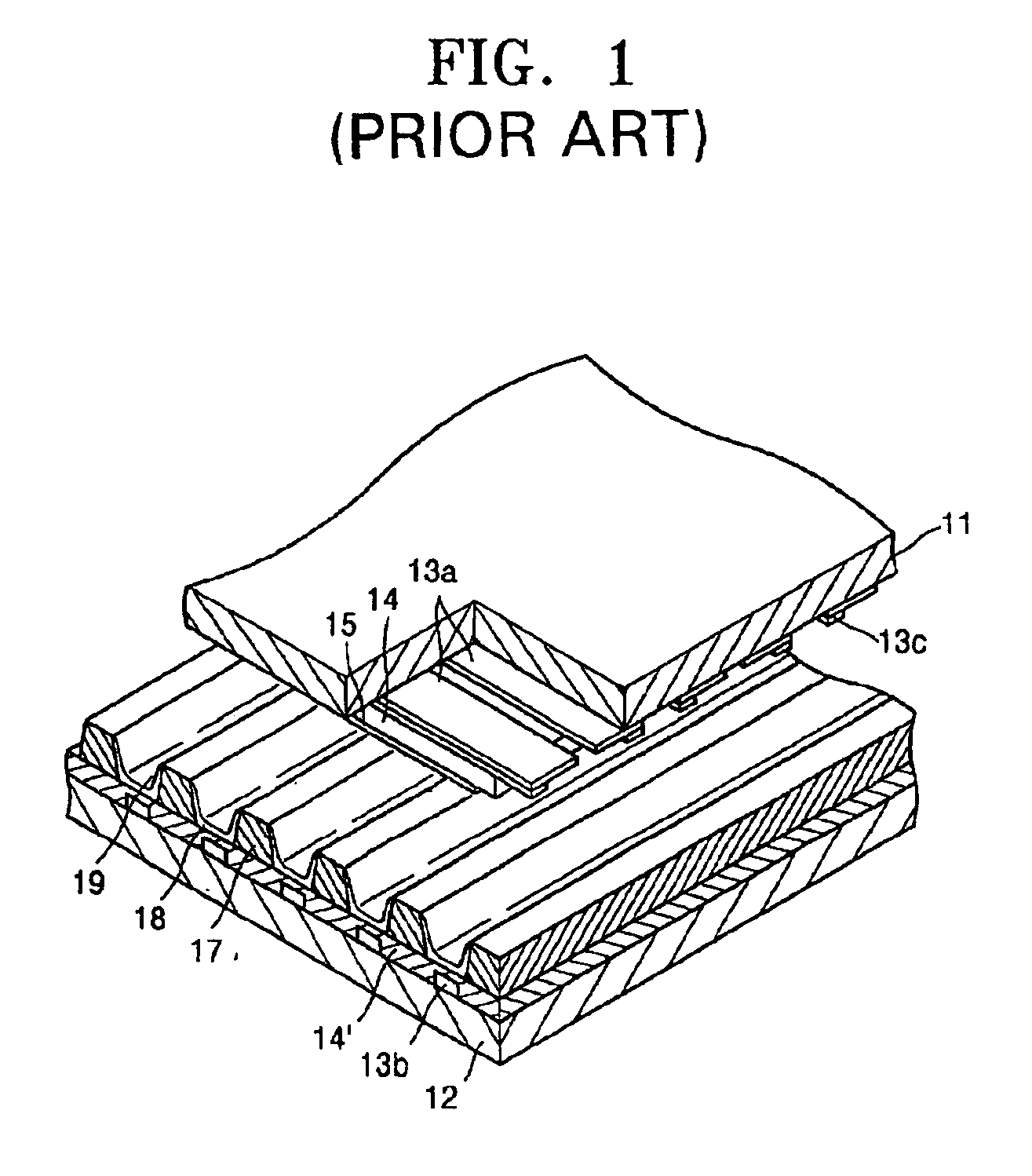
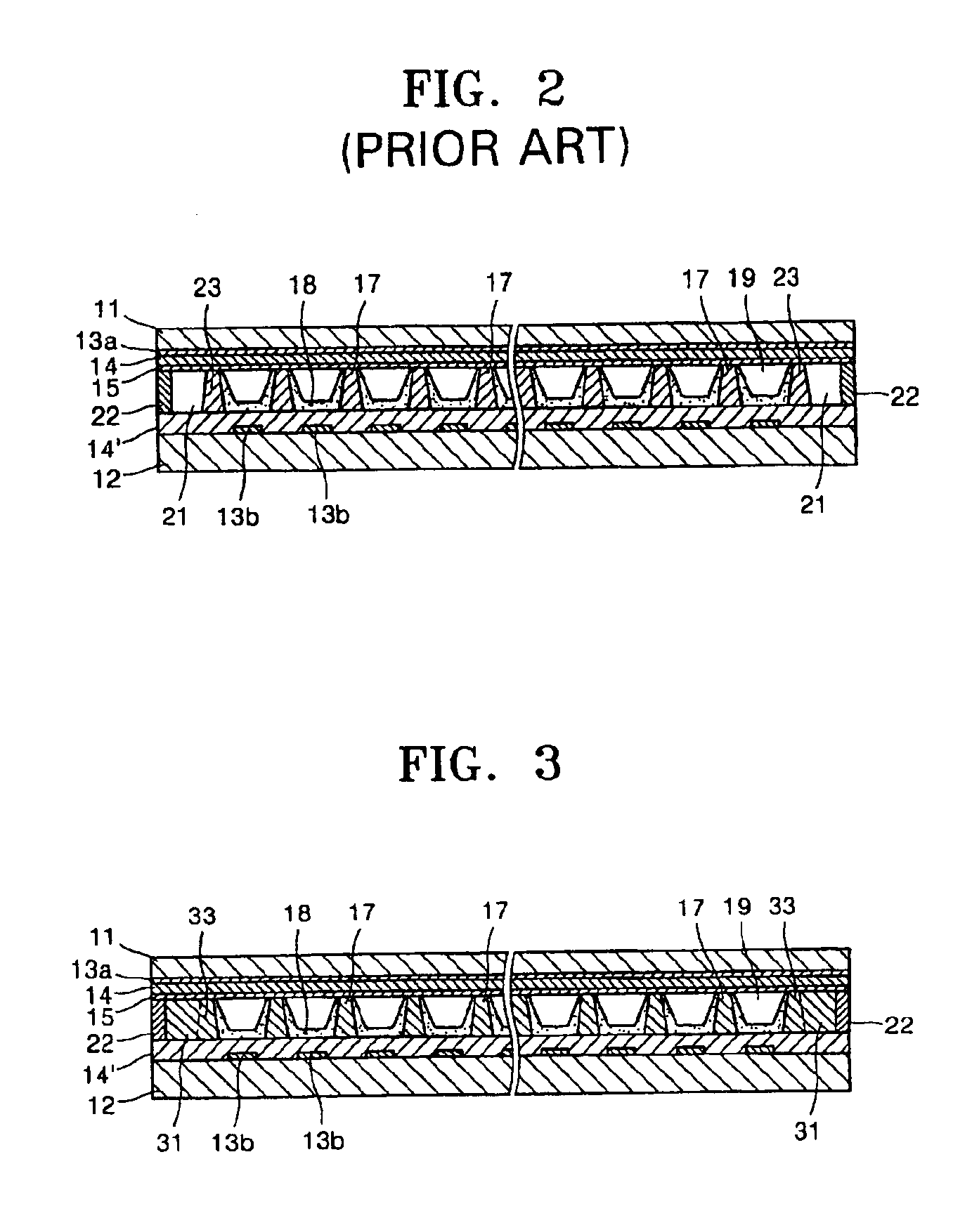
[0037]FIG. 3 shows a cross section in a widthwise direction across partitions 17 of a plasma display panel according to an embodiment of the present invention. The same elements as the plasma display panel of FIG. 2 are indicated by the same reference numerals. Referring to FIG. 3, the first electrode 13a, a third electrode (not shown), the dielectric layer 14, and the protective layer 15 are formed in order on the front glass substrate 11. The second electrode 13b, the dielectric layer 14′, and the partitions 17 are formed in order on the rear glass substrate 12. The front and rear glass substrates 11 and 12 are combined with each other by a...


PUM


Abstract

A plasma display panel includes a front glass substrate and a rear glass substrate coupled to each other by a sealing material coated at edges of the front and rear glass substrates, first and second electrodes disposed perpendicular to each other on opposing inner surfaces of the front and rear glass substrates facing each other, a dielectric layer formed on each of the opposing inner surfaces of the front and rear glass substrates to cover the first and second electrodes, partitions formed on an upper surface of the dielectric layer of the rear glass substrate, red, green and blue fluorescent substances coated between the partitions, and a non-light emitting zone filling portion formed by filling a non-light emitting zone existing between the outermost one of the partitions and the sealing material with a material used for one of the partitions.

Description

CROSS-REFERENCE TO RELATED APPLICATIONS[0001]This application is a continuation of U.S. patent application Ser. No. 09 / 840,290, filed Apr. 24, 2001, now U.S. Pat. No. 6,828,731, which claims the benefit of Korean Application Nos. 00-62873 and 00-21645, filed respectively on Oct. 25, 2000 and Apr. 24, 2000, in the Korean Industrial Property Office, the disclosures of which are incorporated herein by reference.BACKGROUND OF THE INVENTION[0002]1. Field of the Invention[0003]The present invention relates to a plasma display panel and a method of manufacturing partitions thereof, and more particularly, to a plasma display panel in which neon light emission due to mis-discharge in a non-light emitting zone is fundamentally removed, and to a method of manufacturing partitions thereof.[0004]2. Description of the Related Art[0005]A typical plasma display device for displaying an image by using a gas discharge phenomenon is widely noted for its superior display capabilities (display capacity,...

Claims


Application Information

Patent Timeline
Patent Type & Authority Patents(United States)
IPC IPC(8): H01J17/49H01J9/24H01J17/16H01J17/02H01J9/02H01J11/22H01J11/34H01J11/36
CPCH01J9/241H01J9/242H01J11/12H01J11/48H01J11/54H01J11/36H01J2211/368
Inventor KANG, TAE-KYOUNGKIM, KI-JUNG
Owner SAMSUNG SDI CO LTD
Learn More