Focused ion beam endpoint detection using charge pulse detection electronics

a technology of charge pulse and endpoint detection, applied in the direction of individual semiconductor device testing, instruments, nuclear engineering, etc., can solve the problems of electrical malfunction or design flaw, increase in the number of devices, and inability to accurately endpoint, etc., to greatly reduce the success rate of a given device edit operation

Inactive Publication Date: 2005-06-28
TEXAS INSTR INC
View PDF4 Cites 30 Cited by
  • Summary
  • Abstract
  • Description
  • Claims
  • Application Information

AI Technical Summary

Benefits of technology

[0016]The problems noted above are solved in large part by a system and method for determining the endpoint for a focused ion beam (FIB) milling process on an integrated circuit semiconductor sample. The preferred embodiments of the present invention involve using charge pulse detection electronics (CPDE) to monitor the ion-beam-induced current generated while milling a semiconductor sample with a focused ion beam (FIB) apparatus. When an ion from the beam strikes the semiconductor sample, a current transient is generated and fed to the CPDE, which produces a distribution curve on a histogram display as output. The shift in the distribution curve as milling progresses enables close monitoring of the milling process and gives an indication of proximity to the endpoint of the mill. A preferred configuration of the CPDE components includes a charge preamplifier, a pulse amplifier, a pulse shaper, and a multichannel analyzer (MCA).

Problems solved by technology

Metal layers (which typically increase in number as device complexity increases) include patterns of conductive material that are insulated from one another vertically by alternating layers of insulating material.
Periodically, an electrical malfunction or design flaw is found when an integrated circuit is electrically tested.
Imprecise endpointing can greatly reduce the chances of success for a given device edit operation due to the potential of inadvertently creating either opens or shorts in the circuits.
Determining an endpoint for the milling operation, or the instance at which the beam has reached the layer of interest, is becoming more difficult as devices grow in complexity and are designed with a greater number of layers.
Endpoint detection is one of the most difficult tasks with which a failure analyst is faced.
The aforementioned methods may be suitable for surface milling, but on advanced integrated circuits with several metal layers, the relatively high aspect ratios of the complex edits can make it very difficult to obtain sufficient image contrast for precise endpoint detection.
As ports are generally limited on FIBs and may be needed for other operations, port availability can often be an issue.
When the ion beam impacts the surface of the device, a charge build-up occurs when dielectric materials are struck.
Applying a voltage to the conductive layer of interest greatly impacts the secondary yield, and thereby changes the image contrast.
However, provide a wired connection can be a difficult task to achieve when modifying a wafer, i.e., a device that is not packaged.
Applying a voltage directly to the layer of interest within a wafer is much more complicated.
Despite recent advancements, endpoint detection is still one of the most difficult steps in device modification and is often the reason for failures in the FIB edit and modification process.
As devices continue to increase in complexity and number of layers, successful endpoint detection will become even more difficult to achieve.

Method used


Image

  • Focused ion beam endpoint detection using charge pulse detection electronics
  • Focused ion beam endpoint detection using charge pulse detection electronics
  • Focused ion beam endpoint detection using charge pulse detection electronics

Examples


Embodiment Construction

[0029]The following discussion is directed to various embodiments of the invention. Although one or more of these embodiments may be preferred, the embodiments disclosed should not be interpreted, or otherwise used, as limiting the scope of the disclosure, including the claims, unless otherwise specified. In addition, one skilled in the art will understand that the following description has broad application, and the discussion of any embodiment is meant only to be exemplary of that embodiment, and not intended to intimate that the scope of the disclosure, including the claims, is limited to that embodiment.

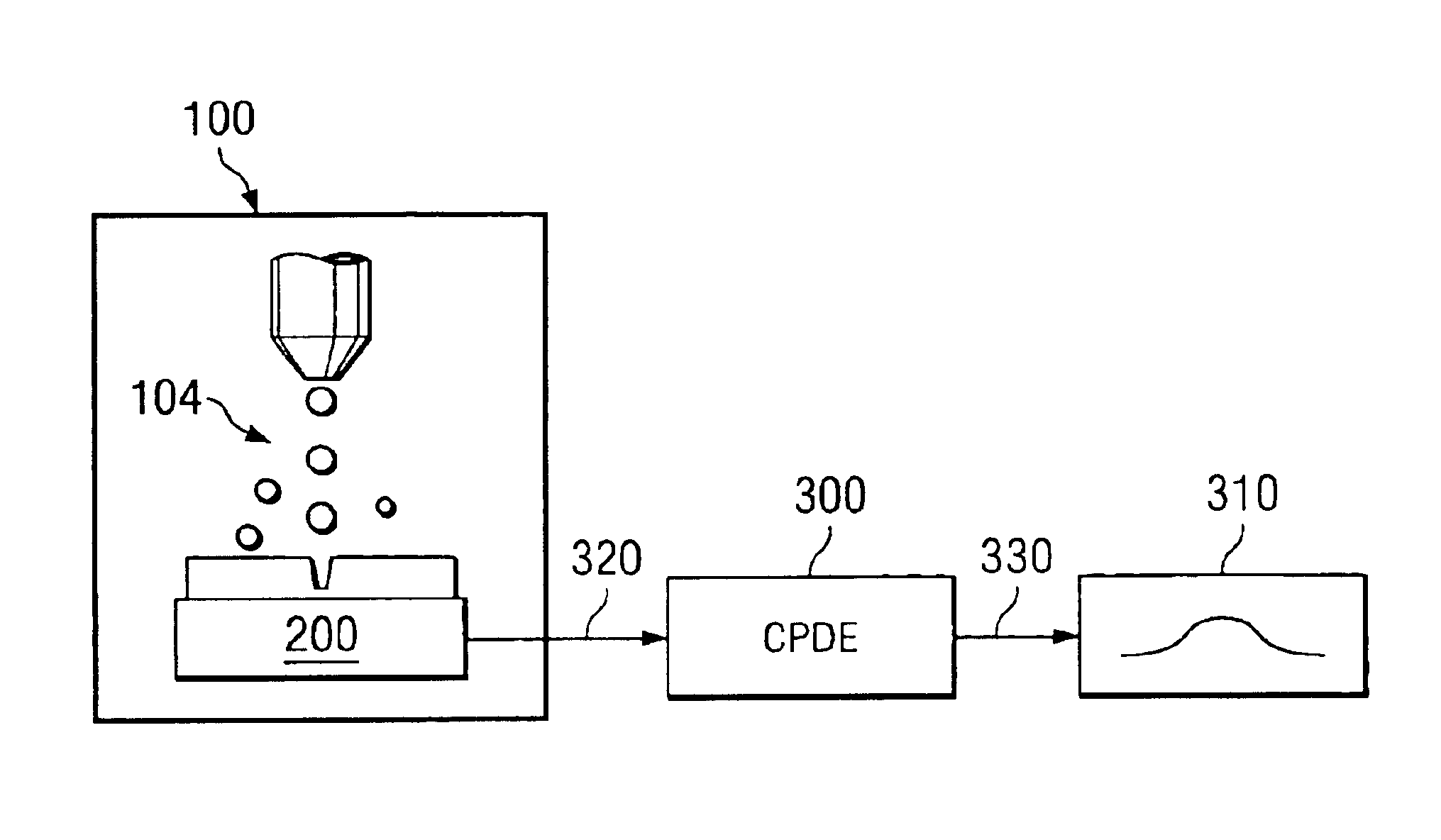
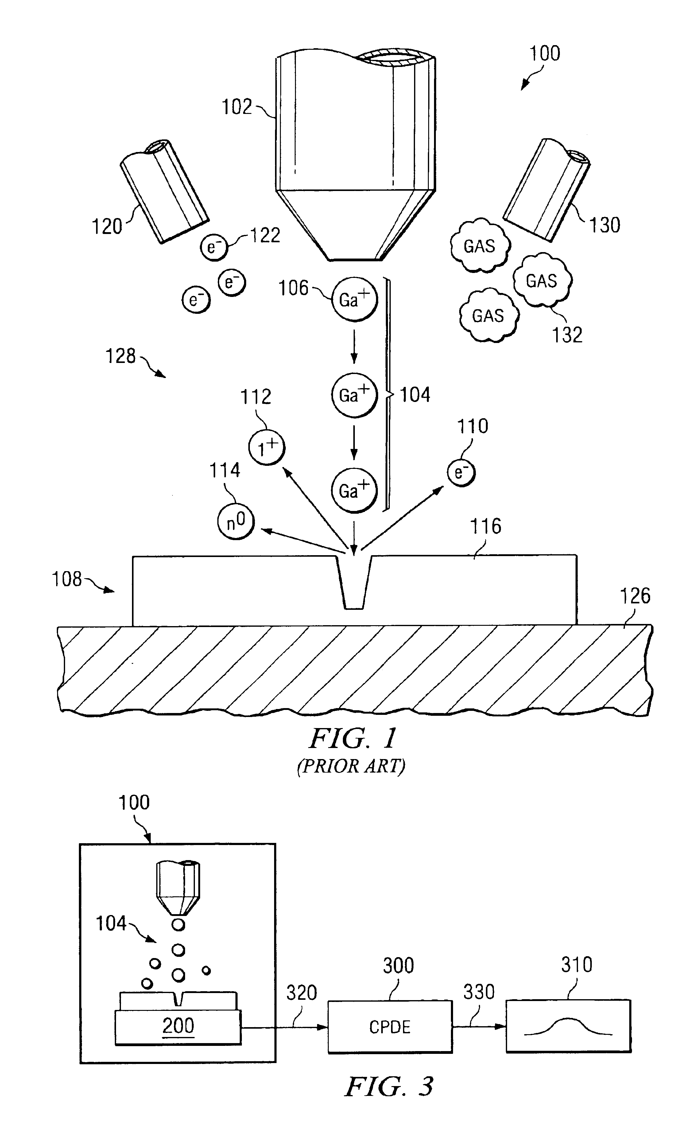
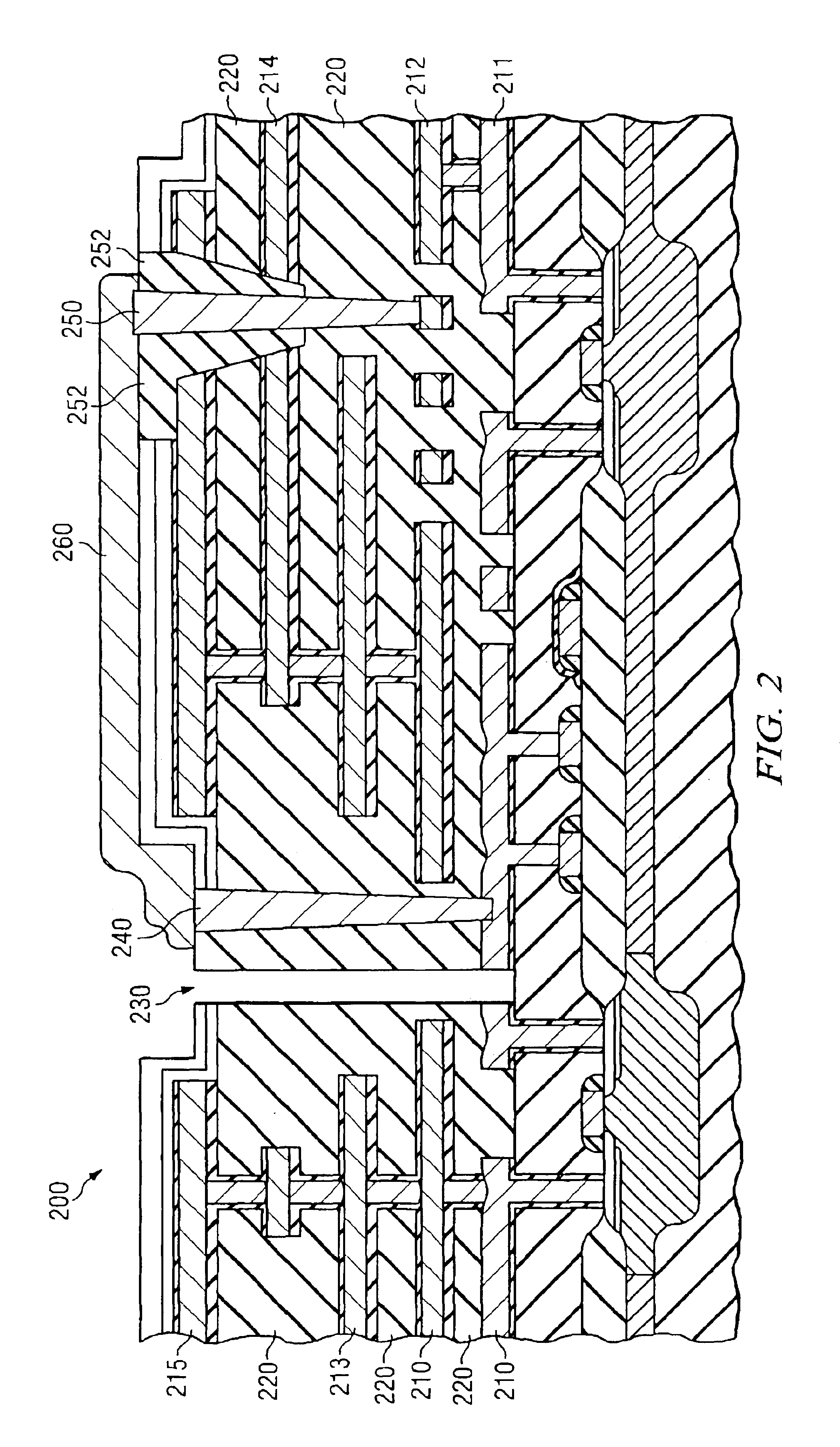
[0030]Disclosed herein is a method for endpoint detection that may used when milling with a focused ion beam (FIB). FIG. 2 shows a cross-sectional view of typical integrated circuit sample 200 with exemplary device modifications formed by an FIB. Integrated circuit 200 includes several metal layers 210, which are conventionally labeled MTn, where n is a layer number commonly desi...


PUM


Abstract

A system and method for detecting a milling endpoint on a semiconductor sample by directing an ion beam from a focused ion beam (FIB) apparatus at the sample and using charge pulse detection electronics (CPDE) components to generate a distribution curve on a histogram display. A preferred configuration of the CPDE components includes a charge preamplifier, a pulse amplifier, a pulse shaper, and a multichannel analyzer (MCA).

Description

BACKGROUND[0001]Integrated circuits, comprised of numerous circuit elements, are typically fabricated in layers on the surface of a semiconductor wafer. Many fabrication processes are repeated numerous times, constructing layer after layer until fabrication is complete. Metal layers (which typically increase in number as device complexity increases) include patterns of conductive material that are insulated from one another vertically by alternating layers of insulating material. Vertical, conductive tunnels called “vias” typically pass through insulating layers to form conductive pathways between adjacent conductive patterns.[0002]Periodically, an electrical malfunction or design flaw is found when an integrated circuit is electrically tested. Implementing a design change can be an extensive process. Typically, among other tasks, a circuit designer may have to produce new schematics, a vendor may need to supply new masks or other fabrication supplies, and wafer fab personnel may ne...

Claims


Application Information

Patent Timeline
Patent Type & Authority Patents(United States)
IPC IPC(8): H01J37/305G01Q40/02G01Q30/04
CPCH01J37/3056H01J2237/30466
Inventor KOLACHINA, SIVARAMAKRISHNAPERUNGULAM, SRIKANTH M.
Owner TEXAS INSTR INC
Why Eureka
Try Eureka