Method of driving anti-ferroelectric liquid crystal display panel for equalizing transmittance of the panel

a technology equalizing transmittance, which is applied in the direction of electric digital data processing, instruments, computing, etc., can solve the problem of uniform display characteristics, and achieve the effect of increasing the reliability of anti-ferroelectric liquid crystal cells selection

Inactive Publication Date: 2005-07-05
SAMSUNG DISPLAY CO LTD
View PDF4 Cites 0 Cited by
  • Summary
  • Abstract
  • Description
  • Claims
  • Application Information

AI Technical Summary

Benefits of technology

[0026]Accordingly, since the state of anti-ferroelectric liquid crystal cells selected during the first driving step is inverted at the beginning of the second driving step, the degree of state c

Problems solved by technology

Accordingly, the display cha

Method used


Image

  • Method of driving anti-ferroelectric liquid crystal display panel for equalizing transmittance of the panel
  • Method of driving anti-ferroelectric liquid crystal display panel for equalizing transmittance of the panel
  • Method of driving anti-ferroelectric liquid crystal display panel for equalizing transmittance of the panel

Examples


Embodiment Construction

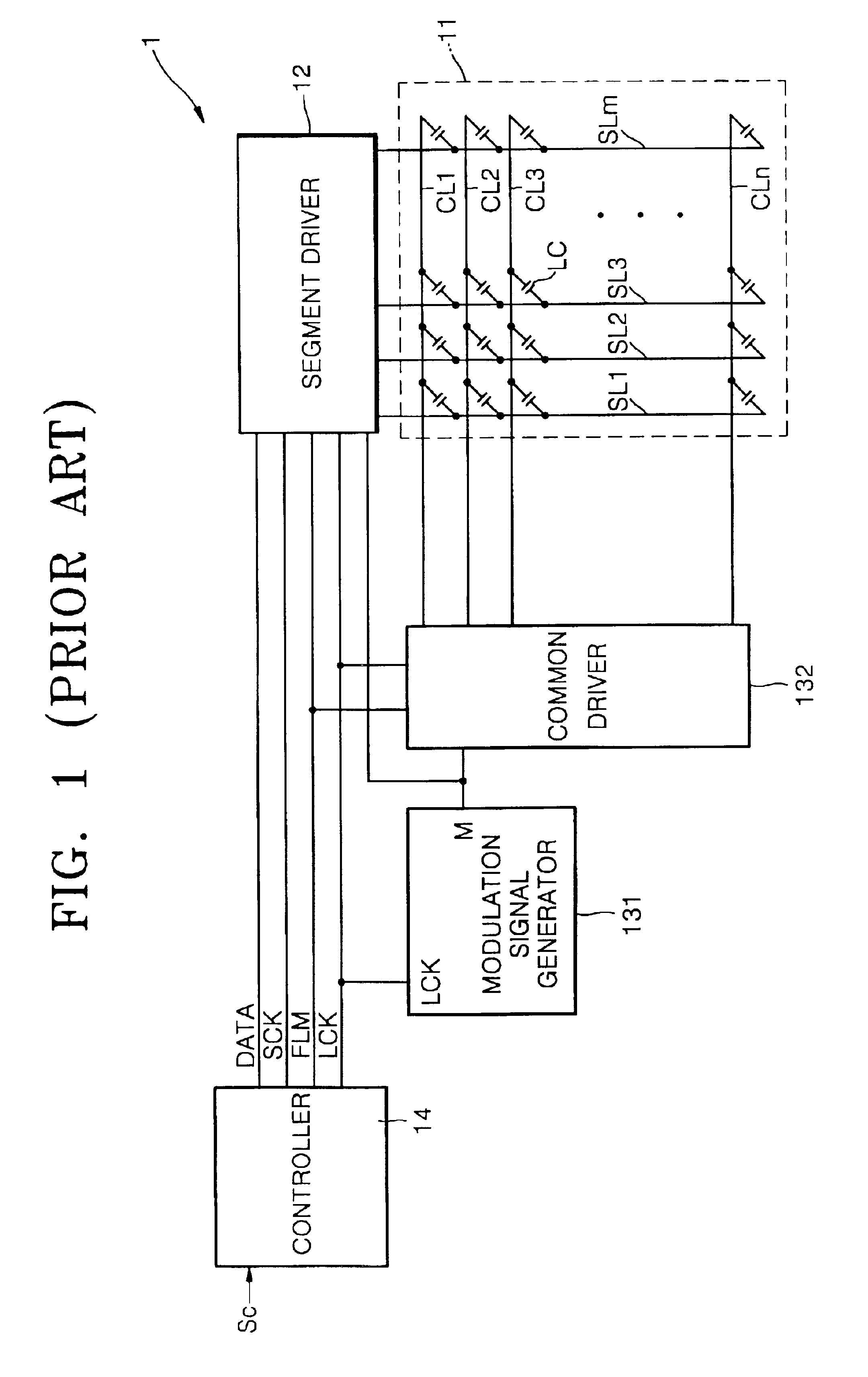
[0034]In an anti-ferroelectric LCD panel to which an embodiment of the present invention is applied, signal electrode lines SL1 through SLm of FIG. 1 are arranged in parallel above anti-ferroelectric liquid crystal cells LC, and scan electrode lines CL1 through CLn are arranged below the anti-ferroelectric liquid crystal cells LC perpendicular to the signal electrode lines SL1 through SLm.

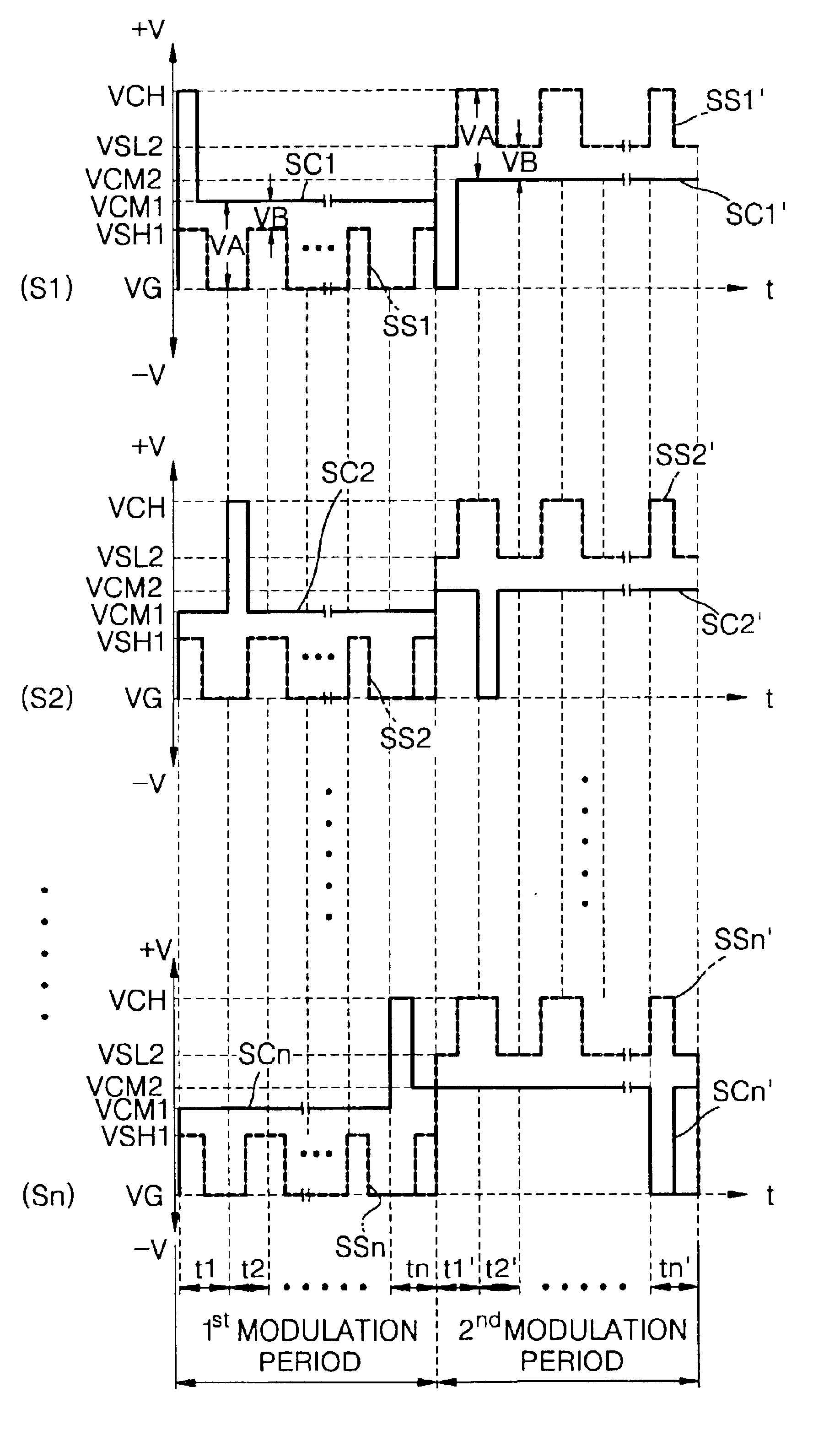
[0035]FIG. 5 shows scan signals SC1, SC2, . . . , SCn, SC1′, SC2′, . . . , SCn′ sequentially applied to the scan electrode lines CL1 through CLn of FIG. 1 and display data signals SS1, SS2, . . . , SSn, SS1′, SS2′, . . . , SSn′ simultaneously applied to the signal electrode lines SL1 through SLm according to an embodiment of the present invention. In FIGS. 3 and 5, the same reference characters denote the same element.

[0036]Referring to FIG. 5, in a first modulation period (from t1 through tn in the case of a waveform S1) corresponding to a first driving step, each of the driving periods (t1 throug...


PUM


Abstract

A method of driving an anti-ferroelectric liquid crystal display (LCD) panel is provided that provides uniform transmittance display characteristics. In the anti-ferroelectric LCD panel, signal electrode lines are arranged in parallel above anti-ferroelectric liquid crystal cells, and at least first and second scan electrode lines are arranged below the anti-ferroelectric liquid crystal cells perpendicular to the signal electrode lines. The method includes a first driving step and a second driving step, which are repeated. Each of the first and second driving steps includes a scanning step, an inversion step, and an iteration step. In the scanning step, a scan selection voltage is applied to the first scan electrode line, and simultaneously, display data signals are applied to the signal electrode lines. In the inversion step, a sustain voltage is applied to the first scan electrode line, and simultaneously, inverted signals of the display data signals which have been applied during the scanning step are applied to the signal electrode lines. In the iteration step, the scanning and inversion steps are repeatedly performed with respect to the second scan electrode line and all of the signal electrode lines.

Description

BACKGROUND OF THE INVENTION[0001]1. Field of the Invention[0002]The present invention relates to a method of driving an anti-ferroelectric liquid crystal display (LCD) panel, and more particularly, to a method for driving an anti-ferroelectric LCD panel having signal electrode lines arranged in parallel above anti-ferroelectric liquid crystal cells, and scan electrode lines arranged in parallel below the anti-ferroelectric liquid crystal cells, perpendicular to the signal electrode lines.[0003]2. Description of the Related Art[0004]Referring to FIG. 1, a general anti-ferroelectric liquid crystal display apparatus 1 includes an anti-ferroelectric LCD panel 11 and a driving unit.[0005]In the anti-ferroelectric LCD panel 11, signal electrode lines SL1, SL2, SL3, . . . , SLm are arranged in parallel above anti-ferroelectric liquid crystal cells LC, and scan electrode lines CL1, CL2, CL3, . . . , CLn are arranged below the anti-ferroelectric liquid crystal cells LC, perpendicular to the ...

Claims


Application Information

Patent Timeline
IPC IPC(8): G09G3/36
CPCG09G3/3633G09G2310/06G09G2320/0233G09G3/36
Inventor YOO, JEONG-GUENPARK, SUNG-CHON
Owner SAMSUNG DISPLAY CO LTD
Why Eureka
Try Eureka