Ball grid array package and process for manufacturing same

a grid array and array technology, applied in the direction of semiconductor devices, semiconductor/solid-state device details, electrical devices, etc., can solve the problems of poor thermal dissipation in the package, low thermal dissipation performance, package suffers disadvantages, etc., to reduce mold flash, improve signal layout on the substrate, and inhibit mold flash

Inactive Publication Date: 2006-01-17
UTAC HEADQUARTERS PTE LTD
View PDF49 Cites 126 Cited by
  • Summary
  • Abstract
  • Description
  • Claims
  • Application Information

AI Technical Summary

Benefits of technology

[0012]A thermal path is provided from the semiconductor die, through the die adapter and the collapsible spacer and to the heat spreader. Also, the heat spreader is effectively pressed against the lower mold die surface during molding, thereby inhibiting mold flash on the outer side of the heat spreader. The incorporation of a deformable material (collapsible spacer) that is stable at molding temperature, provides a compliant layer between the substrate and the heat spreader and the between the semiconductor die and the heat spreader. Thus, the heat spreader is pressed against the lower mold die, maintaining the heat spreader in contact with the lower mold die during molding and reducing mold flash.
[0013]In another aspect, ground bonds are provided between the semiconductor die and the die adapter. Thus, a ground path from is provided through the die adapter, the collapsible spacer in contact with the die adapter, the heat spreader and the collapsible spacers in contact with the substrate. Advantageously, better signal layout on the substrate can be achieved and better wire looping control is provided. Also, ground wire length is reduced.

Problems solved by technology

However, typical PBGA packages include a convoluted signal path, giving rise to high impedance and an inefficient thermal path which results in low thermal dissipation performance.
Because of the absence of a thermal path away from the semiconductor die 24, thermal dissipation in this package is poor.
This package suffers disadvantages, however, as heat must be dissipated from the semiconductor die 24, through the molding compound 28 and then through the heat spreader 32.

Method used


Image

  • Ball grid array package and process for manufacturing same
  • Ball grid array package and process for manufacturing same
  • Ball grid array package and process for manufacturing same

Examples


Embodiment Construction

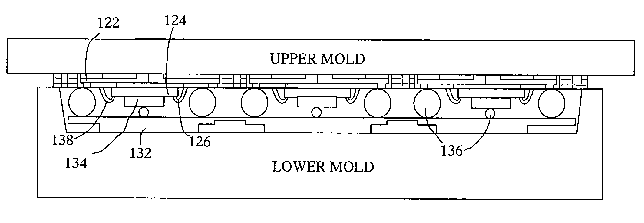
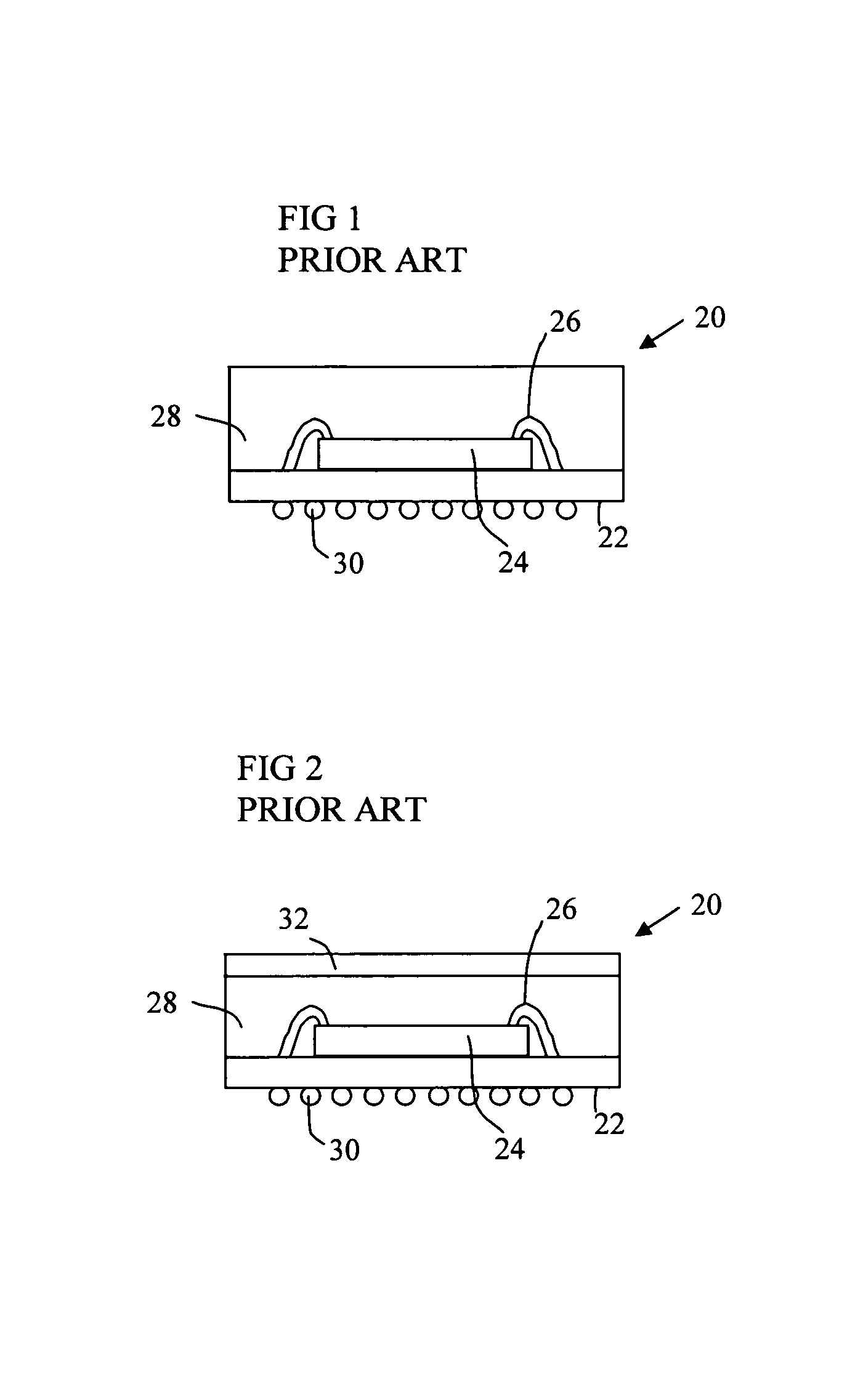
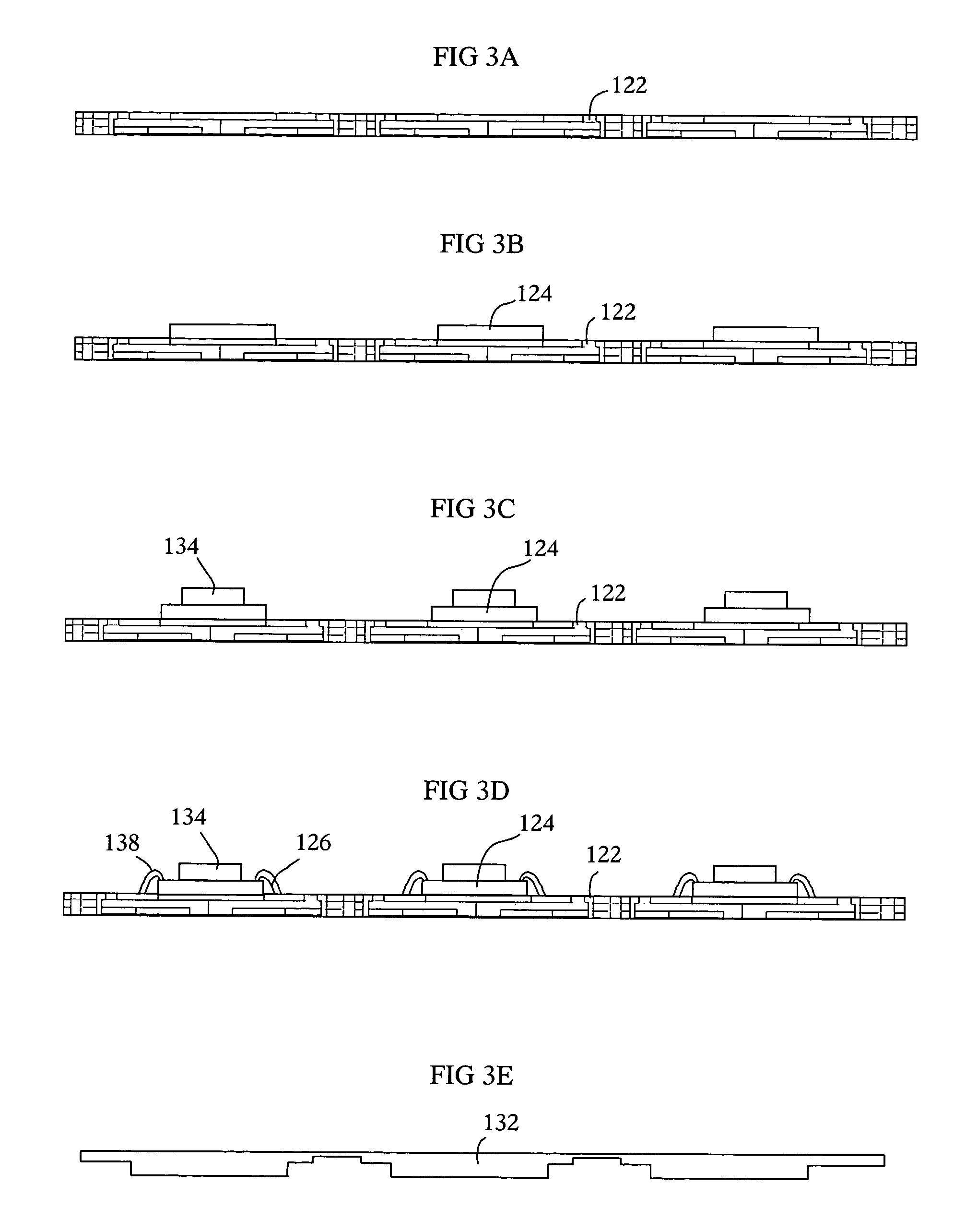
[0022]Reference is now made to FIGS. 3A to 3K to describe a process for manufacturing a ball grid array package, according to an embodiment of the present invention. To simplify the description, the numerals used previously in describing FIG. 1 will be used again after raising the numerals by 100 where parts to be described correspond to parts already described.

[0023]Referring to FIG. 3K, the ball grid array package is indicated generally by the numeral 120. The package 120 includes a substrate 122 that has a plurality of conductive traces. A semiconductor die 124 is mounted to a first surface of the substrate 122 and a die adapter 134 is mounted to the semiconductor die 124. A plurality of wire bonds 126 connect the semiconductor die 124 and ones of the conductive traces. A heat spreader 132 is disposed proximal to and spaced from the die adapter 134 by at least one collapsible spacer 136. A molding compound 128 encapsulates the semiconductor die 124, the wire bonds 126, the die ad...


PUM


Abstract

A ball grid array package is manufactured by mounting a semiconductor die to a first surface of a substrate and mounting a die adapter to the semiconductor die. The semiconductor die is wire bonded to ones of conductive traces of the substrate. A collapsible spacer is mounted to the substrate and the substrate is releasably clamped to an upper side of a mold cavity. A heat spreader and at least one collapsible spacer are placed in the mold cavity such that the collapsible spacer is disposed between the heat spreader and the substrate. A molding compound is molded in the mold, thereby molding the semiconductor die, the substrate, the wire bonds, the die adapter, the at least one collapsible spacer and the heat spreader into the molding compound to provide a molded package. A ball grid array is formed on a second surface of the substrate, bumps of the ball grid array being electrically connected to the conductive traces and the integrated circuit package is singulated.

Description

CROSS REFERENCE TO RELATED APPLICATION[0001]This is a continuation-in-part of co-pending U.S. patent application Ser. No. 10 / 323,657 entitled, Process For Manufacturing Ball Grid Array Package, filed Dec. 20, 2002, which is a continuation-in-part of U.S. patent application Ser. No. 10 / 197,832 entitled Improved Ball Grid Array Package, filed Jul. 19, 2002 now U.S. Pat. No. 6,800,948.FIELD OF THE INVENTION[0002]The present invention relates in general to integrated circuit packaging, and in particular to an improved ball grid array package with enhanced thermal characteristics and a unique method of manufacturing the ball grid array package.BACKGROUND OF THE INVENTION[0003]High performance integrated circuit (IC) packages are well known in the art. Improvements in IC packages are driven by industry demands for increased thermal and electrical performance and decreased size and cost of manufacture.[0004]In general, array packaging such as Plastic Ball Grid Array (PBGA) packages provide...

Claims


Application Information

Patent Timeline
Patent Type & Authority Patents(United States)
IPC IPC(8): H01L21/58H01L23/055H01L23/24H01L23/433
CPCH01L21/561H01L23/055H01L23/16H01L23/24H01L23/3128H01L23/34H01L23/433H01L23/4334H01L23/49816H01L24/97H01L21/563H01L2224/45144H01L2224/32245H01L2224/32225H01L2224/16225H01L2924/01033H01L24/48H01L2924/3011H01L2924/15331H01L2924/15311H01L2924/14H01L2924/01079H01L2924/01047H01L2924/01029H01L2924/01027H01L2924/01013H01L2924/01002H01L2224/97H01L2224/81815H01L2224/8121H01L2224/73253H01L24/81H01L2224/16H01L2224/48091H01L2224/48227H01L2224/73204H01L2924/00014H01L2224/81H01L2924/00012H01L2924/00H01L2924/181H01L24/45H01L2924/00015H01L2224/05599
Inventor FAN, CHUN HOLAM, WING KEUNGSZE, MING WANGLABEEB, SADAK THAMBYMCLELLAN, NEILKIRLOSKAR, MOHAN
Owner UTAC HEADQUARTERS PTE LTD
Why Eureka
Try Eureka