Process for manufacturing ball grid array package

a technology of grid array and manufacturing process, which is applied in the direction of semiconductor devices, semiconductor/solid-state device details, electrical apparatus, etc., can solve the problems of poor thermal dissipation and low thermal dissipation performance of this package, and achieve the effect of reducing mold flash

Inactive Publication Date: 2005-12-27
UTAC HEADQUARTERS PTE LTD
View PDF49 Cites 94 Cited by
  • Summary
  • Abstract
  • Description
  • Claims
  • Application Information

AI Technical Summary

Benefits of technology

[0011]In another aspect, a die adapter is included, the die adapter is mounted to the semiconductor die and contacts the upper surface of the heat spreader during molding to provide a package with a direct thermal path from the semiconductor die through the die adapter, to the heat spreader. The die adapter effectively pins the heat spreader against the lower mold surface during molding, thereby aiding in reducing mold flash on the outer side of the heat spreader.

Problems solved by technology

However, typical PBGA packages include a convoluted signal path, giving rise to high impedance and an inefficient thermal path which results in low thermal dissipation performance.
Because of the absence of a thermal path away from the semiconductor die, thermal dissipation in this package is poor.

Method used


Image

  • Process for manufacturing ball grid array package
  • Process for manufacturing ball grid array package
  • Process for manufacturing ball grid array package

Examples


Embodiment Construction

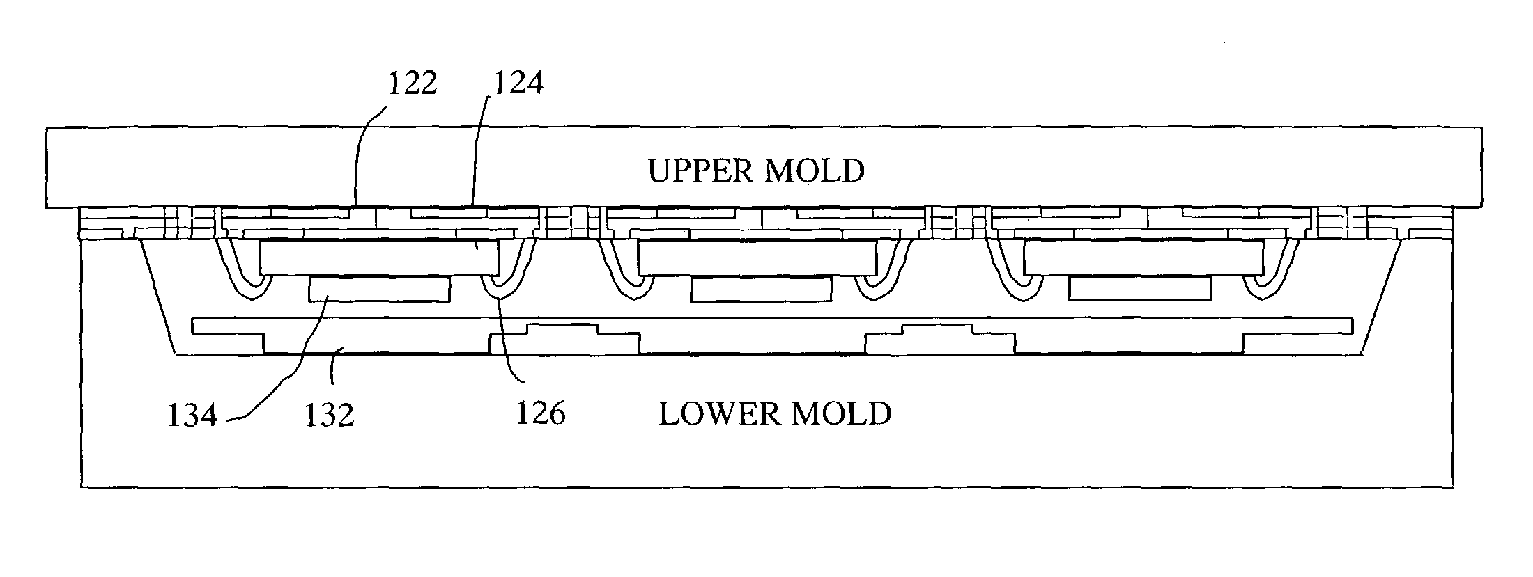
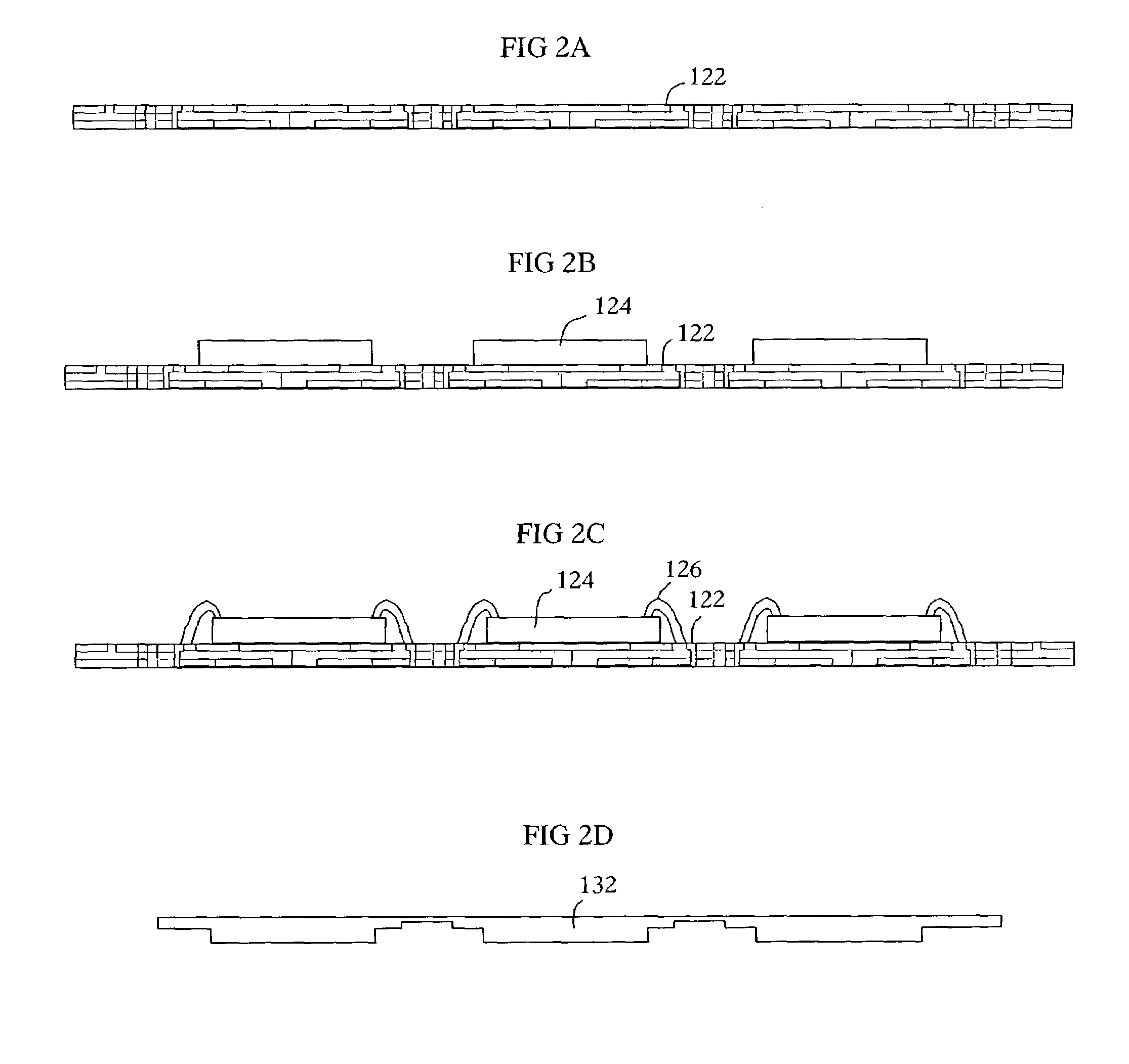
[0020]Reference is now made to FIGS. 2A to 2H to describe a process for manufacturing a ball grid array package, according to an embodiment of the present invention. To simplify the description, the numerals used previously in describing FIG. 1 will be used again after raising the numerals by 100 where parts to be described correspond to parts already described.

[0021]The ball grid array package is indicated generally by the numeral 120 and is manufactured by mounting a semiconductor die 124 to a first surface of a substrate array 122. Wires 126 are bonded between the semiconductor die 124 and ones of conductive traces of the substrate array 122. The heat spreader 132 is disposed in a mold cavity and the substrate array 122 is releasably clamped to a topside of the mold. The semiconductor die 124, the substrate array 122, the wire bonds 126 and the heat spreader 132 are molded into a molding material to provide a molded package. Next, the molded package is removed from the mold and a...


PUM


Abstract

A ball grid array package is manufactured by mounting a semiconductor die to a first surface of a substrate array. Wires are bonded between the semiconductor die and ones of conductive traces of the substrate array. The heat spreader is disposed in a mold and the substrate array is releasably clamped to a top die of the mold. The semiconductor die, the substrate array, the wire bonds and the heat spreader are molded into a molding material to provide a molded package. Next, the molded package is removed from the mold and a plurality of solder balls are added in the form of a ball grid array on a second surface of the substrate array such that bumps of the ball grid array are electrically connected to the conductive traces. The integrated circuit package is then singulated from a remainder of the substrate array.

Description

CROSS REFERENCE TO RELATED APPLICATION[0001]This is a continuation-in-part of U.S. patent application Ser. No. 10 / 197,832 entitled Improved Ball Grid Array Package, filed Jul. 19, 2002, now U.S. Pat. No. 6,800,948.FIELD OF THE INVENTION[0002]The present invention relates in general to integrated circuit packaging, and in particular to a unique method of manufacture of a ball grid array package with enhanced thermal characteristics.BACKGROUND OF THE INVENTION[0003]High performance integrated circuit (IC) packages are well known in the art. Improvements in IC packages are driven by industry demands for increased thermal and electrical performance and decreased size and cost of manufacture.[0004]In general, array packaging such as Plastic Ball Grid Array (PBGA) packages provide a high density of interconnects relative to the surface area of the package. However, typical PBGA packages include a convoluted signal path, giving rise to high impedance and an inefficient thermal path which r...

Claims


Application Information

Patent Timeline
Patent Type & Authority Patents(United States)
IPC IPC(8): H01L21/44H01L21/56H01L21/68H01L23/31H01L23/433H01L23/498
CPCH01L21/561H01L21/568H01L21/6835H01L23/3128H01L23/4334H01L24/97H01L23/49816H01L2224/16H01L2224/48091H01L2224/48247H01L2224/97H01L2924/01029H01L2924/01046H01L2924/01047H01L2924/01078H01L2924/01079H01L2924/01082H01L2924/14H01L2924/15311H01L2924/3011H01L2224/85H01L2924/00014H01L24/48H01L2924/01033H01L2224/45144H01L2924/00H01L2224/48227H01L2224/73265H01L2924/181H01L24/45H01L2924/18165H01L2224/2612H01L2924/00015H01L2924/00012
Inventor FAN, CHUN HOLABEEB, SADAK THAMBYSZE, MING WANG
Owner UTAC HEADQUARTERS PTE LTD
Why Eureka
Try Eureka