In-plane switching mode liquid crystal display device and method for fabricating the same

Active Publication Date: 2006-02-14
LG DISPLAY CO LTD
View PDF3 Cites 8 Cited by
  • Summary
  • Abstract
  • Description
  • Claims
  • Application Information

AI Technical Summary

Benefits of technology

[0025]Accordingly, a contact hole forming process for an electrical connection between the source/drain electrode and the channel layer and for an electrical connection between the pixel electrode and the drain electrode, can be integrated as

Problems solved by technology

However, this method has a problem that a viewing angle is as narrow as 90°.
However, the field effect mobility of the amorphous silicon thin film transistor of about (2/Vsec) prevents its use in peripheral circuits that apply signals to the pixel region, because the peripheral circuits operate at more than 1 MHz.
Therefore, the channel layer is electrically and optically influenced by the backlight, which may cause an off-current, namely, a leakage current to be incr

Method used


Image

  • In-plane switching mode liquid crystal display device and method for fabricating the same
  • In-plane switching mode liquid crystal display device and method for fabricating the same
  • In-plane switching mode liquid crystal display device and method for fabricating the same

Examples


Example

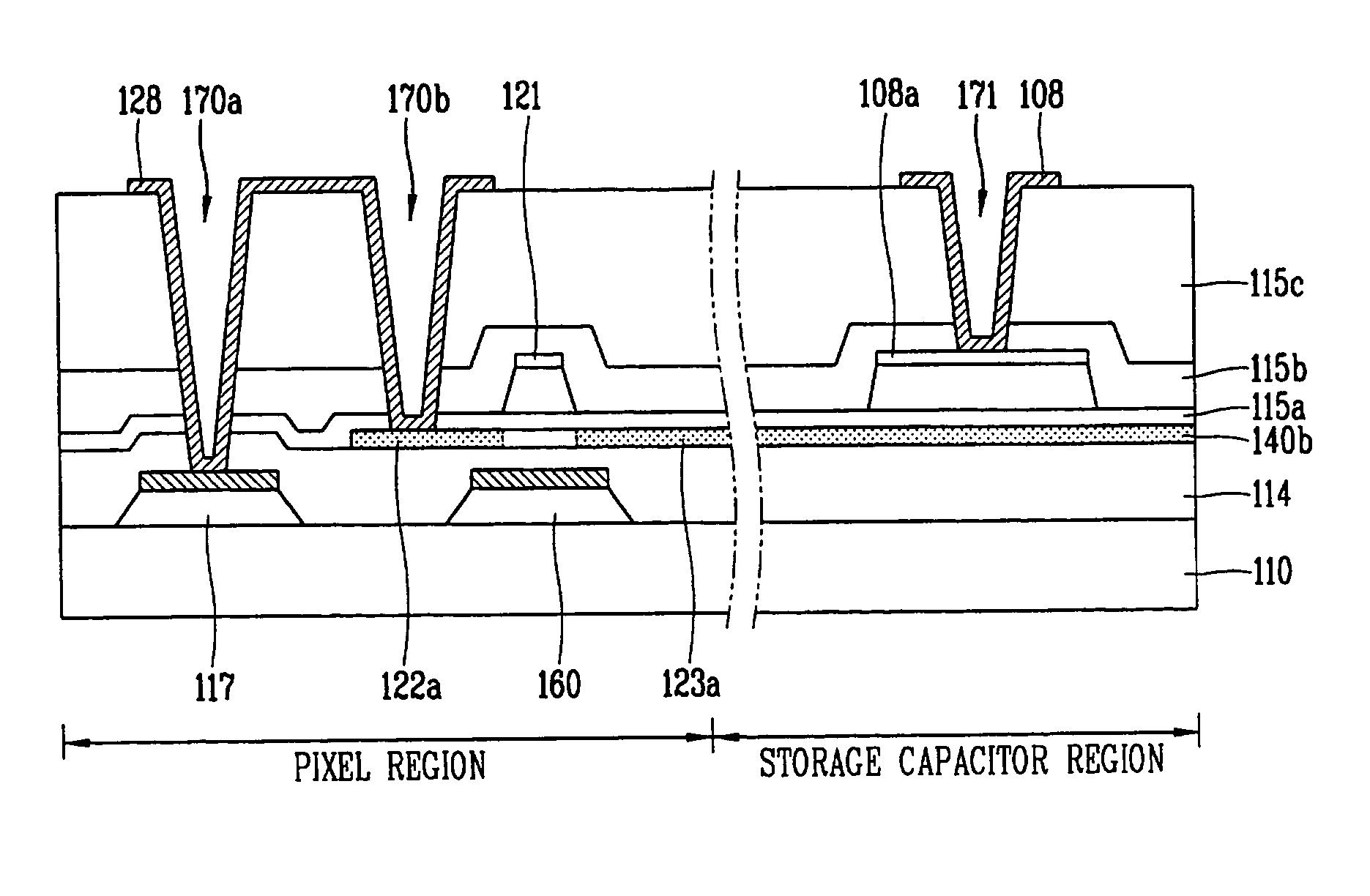
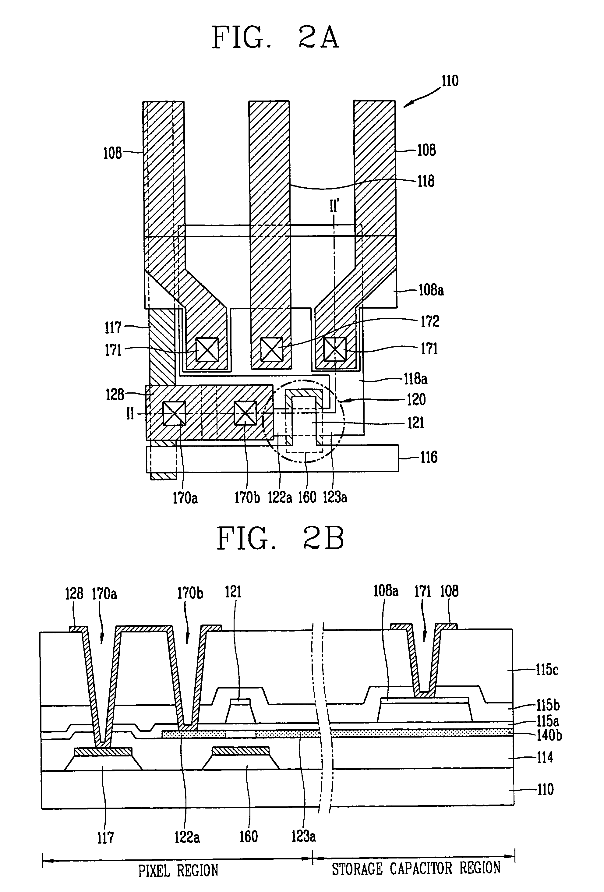
[0068]The in-plane switching LCD device according to the second embodiment has the same construction as that according to the first embodiment of FIG. 2 except the pixel electrode forming method.

[0069]As shown in FIG. 4, an array substrate 210 includes a gate line 216 and a data line 217 for defining a pixel region by being arranged vertically and horizontally thereon, and a thin film transistor 220 formed at the intersection region between the gate line 216 and the data line 217 as a switching device.

[0070]A light-shielding layer 260 is formed below a channel layer (not shown) of the thin film transistor 220 for preventing light of a lower backlight from being introduced into the channel layer.

[0071]At least one pair of common electrodes 208 and pixel electrodes 218 for generating an in-plane horizontal electric field are alternately arranged in the pixel region. The common electrode 208 is electrically connected to a common electrode line 208a disposed parallel to the gate line 21...

Example

[0072]Unlike the first embodiment, in the second embodiment, the pixel electrode 218 is formed of the same polycrystalline silicon thin film as the pixel electrode line 218a, so that the third contact hole for electrically connecting the pixel electrode 218 with the pixel electrode line 218a is not required. As the result, a contact hole can be reduced by one per one pixel, thereby minimizing the contact inferiority.

[0073]The common electrode line 208a is formed on the same plane as the gate line 216, and the pixel electrode line 218a is formed on the same plane as the data region 223a. A first insulating layer is disposed between the common electrode line 208a and the pixel electrode line 218a thus to constitute a storage capacitor.

[0074]FIG. 5 is a plane view showing a part of an array substrate for an in-plane switching LCD device according to a third embodiment.

Example

[0075]The in-plane switching LCD device according to the third embodiment has the same construction as that according to the first embodiment of FIGS. 2A, 2B except the method for forming the pixel electrode and common electrode.

[0076]Unlike the first embodiment, in the third embodiment, the pixel electrode is formed of the polycrystalline silicon thin film and the common electrode is formed together with the common electrode line, so that the second contact hole and the third contact hole are not required.

[0077]As shown in FIG. 5, an array substrate 310 comprises a gate line 316 and a data line 317 for defining a pixel region by being arranged vertically and horizontally thereon, and a thin film transistor 320 formed at the intersection region between the gate line 316 and the data line 317 as a switching device.

[0078]A light-shielding layer 360 is formed below a channel layer (not shown) of the thin film transistor 320 for preventing light of a lower backlight from being introduce...


PUM


Abstract

A method for fabricating an in-plane switching LCD device includes forming a data line and a light-shielding layer on a substrate, forming a pixel electrode line and an active region with a polycrystalline silicon thin film, forming a first insulating layer on the substrate, forming a gate electrode and a common electrode line on the first insulating layer, forming a second insulating layer on the substrate, forming a first contact hole that exposes at least portions of the data line and the active region, and forming a connection electrode that connects at least portions of the exposed data line and the active region.

Description

[0001]This application claims the benefit of Korean Patent Application No. 2003-042833, filed on Jun. 27, 2003, which is hereby incorporated by reference.BACKGROUND OF THE INVENTION[0002]1. Field of the Invention[0003]The present invention relates to a liquid crystal display (LCD) device, and more particularly, to an in-plane switching mode LCD device, and a method for fabricating the same.[0004]2. Discussion of the Related Art[0005]Recently, with the increase of the need for displaying information and the demand for using portable information systems, light and thin film type flat panel display (FPD) devices have been actively researched and commercialized, and the conventional cathode ray tube (CRT) devices have been replaced. Among these flat panel display devices, an LCD device is utilized for displaying an image by utilizing an optical anisotropy of a liquid crystal. The LCD device can be installed in a notebook computer, a desktop monitor, or any other display devices because ...

Claims


Application Information

Patent Timeline
IPC IPC(8): H01L21/00G02F1/1343G02F1/136G02F1/1362G09F9/30G09F9/35H01L21/77H01L29/786
CPCG02F1/134363G02F1/136213H01L27/124G02F2202/104H01L29/78633G02F1/136227G02F1/136
Inventor KIM, BYEONG KOOHA, YONG MINJEOUNG, HUN
Owner LG DISPLAY CO LTD
Why Eureka
Try Eureka