Semiconductor storage device

Inactive Publication Date: 2006-02-14
KK TOSHIBA
View PDF3 Cites 45 Cited by
  • Summary
  • Abstract
  • Description
  • Claims
  • Application Information

AI Technical Summary

Benefits of technology

[0010]FIG. 1 is a view showing a conventional countermeasure

Problems solved by technology

A problem has become prominent in that leakage current increases in memory cells on standby, as a consequence of the reduced size and operation voltage of LSIs.
As a consequence, leakage current tunneling through the gate oxide film (gate leakage) increases and thereb

Method used


Image

  • Semiconductor storage device
  • Semiconductor storage device
  • Semiconductor storage device

Examples


first embodiment

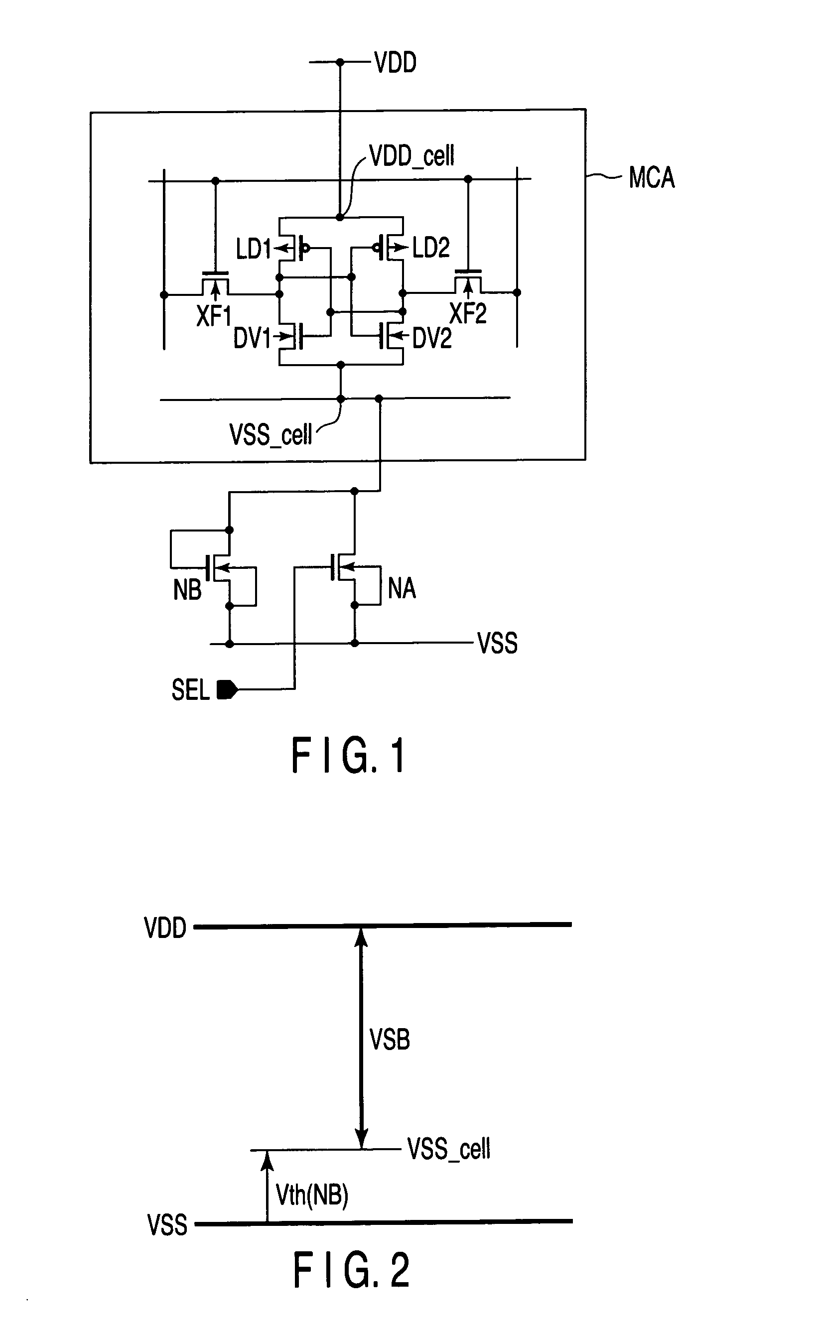
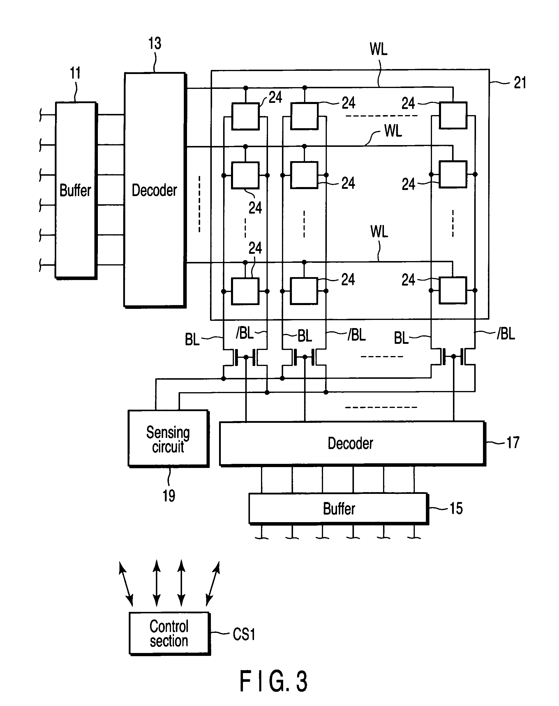
[0032]FIG. 3 is a block diagram showing an SRAM (semiconductor storage device) according to a first embodiment of the present invention. The SRAM includes a memory cell array 21, in which memory cells 24 are respectively disposed at addresses arrayed in a matrix format. Word lines WL for selecting the memory cells are respectively connected to the rows of the memory cell array 21. Complementary pairs of data lines BL and / BL for transmitting data to and from the memory cells are respectively connected to the columns of the memory cell array 21.

[0033]A row address buffer 11 and a row decoder 13 are disposed to select the word lines WL. A column address buffer 15 and a column decoder 17 are disposed to select the data lines BL and / BL. A sensing circuit 19 is connected to the data lines BL and / BL, for reading stored data. The row address buffer 11 and column address buffer 12 are connected to a control section CS1 for generating address signals, data signals, and so forth. The contro...

second embodiment

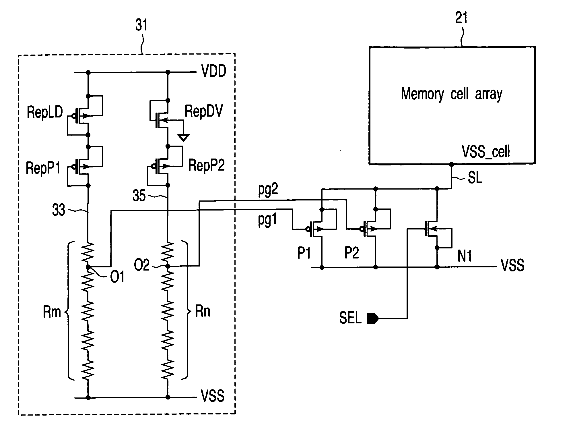
[0058]FIG. 7 is a view showing an SRAM (semiconductor storage device) according to a second embodiment of the present invention, focusing on circuitry for clamping the standby voltage thereof. The SRAM according to the second embodiment has the same structure as the SRAM according to the first embodiment except the bias generator.

[0059]As shown in FIG. 7, the bias generator 41 of this SRAM includes two paths (i.e. two bias generation circuits) 43 and 45, each of which is supplied with the power supply potential VDD and ground potential VSS at opposite ends. The first path 43 is provided with a transistor group RepLDA, a transistor group RepLDB, a transistor RepP1, and a plurality of resistors Rm disposed thereon in series, in this order from the end supplied with the power supply potential VDD. The second path 45 is provided with a transistor group RepDVA, a transistor group RepDVB, a transistor RepP2, and a plurality of resistors Rn disposed thereon in series, in this order from th...

third embodiment

[0064]FIG. 8 is a view showing an SRAM (semiconductor storage device) according to a third embodiment of the present invention, focusing on circuitry for clamping the standby voltage thereof. The SRAM according to the third embodiment has the same structure as the SRAM according to the first embodiment except the bias generator.

[0065]As shown in FIG. 8, the bias generator 51 of this SRAM further includes a current mirror circuit 53 to supply a constant current regardless of fluctuations in the power supply potential VDD. The current mirror circuit 53 is connected in parallel with two paths (i.e. two bias generation circuits) 33 and 35. The path of the current mirror circuit 53 is provided with a transistor 55 disposed thereon, whose gate terminal is connected to a constant potential source to avoid any influence caused by fluctuations in the power supply potential VDD. With this arrangement, bias potentials pg21 and pg22 outputted from the bias generator 51 can be more stable.


PUM


Abstract

A semiconductor storage device includes first and second additional FETs disposed in parallel on one of potential lines for supplying first and second drive potentials to each SRAM memory cell. When each memory cell is selected, a selection signal is supplied to the gate terminal of the first additional FET through a selection signal supply line to turn on the first additional FET. A bias generation circuit is configured to generate a bias potential and supply it to the gate terminal of the second additional FET. The bias potential is generated to reflect one or both of fluctuations in the potential difference between the first and second drive potentials, and variations in the threshold voltage of FETs included in the cross-feedback circuit of each memory cell.

Description

CROSS-REFERENCE TO RELATED APPLICATIONS[0001]This application is based upon and claims the benefit of priority from the prior Japanese Patent Application No. 2004-253221, Aug. 31, 2004, the entire contents of which are incorporated herein by reference.BACKGROUND OF THE INVENTION[0002]1. Field of the Invention[0003]The present invention relates to a semiconductor storage device, and particularly to a technique for reducing standby current in a static semiconductor storage device, e.g., an SRAM (SRAM: Static Random Access Memory).[0004]2. Description of the Related Art[0005]SRAMs (typically, each memory cell includes six transistors to store one bit) are widely used for LSIs (LSI: Large Scale Integrated circuit). A problem has become prominent in that leakage current increases in memory cells on standby, as a consequence of the reduced size and operation voltage of LSIs. The term “standby” means that a memory cell is in the non-selected state.[0006]The thickness of the gate oxide film...

Claims


Application Information

Patent Timeline
IPC IPC(8): G11C7/00
CPCG11C11/413G11C5/147G11C5/148G11C11/417
Inventor HIRABAYASHI, OSAMU
Owner KK TOSHIBA
Why Eureka
Try Eureka