Split gate memory cell for programmable circuit device

a memory cell and circuit device technology, applied in the field of memory cells, can solve the problems of significantly higher voltages that are necessary to program and erase the memory device, subject to the art solution, etc., and achieve the effects of compact cell size, reduced stand-by leakage, and low on-state switch impedan

Active Publication Date: 2010-04-06
MICROSEMI SOC
View PDF67 Cites 25 Cited by
  • Summary
  • Abstract
  • Description
  • Claims
  • Application Information

AI Technical Summary

Benefits of technology

[0007]According to a first aspect of the present invention, a split-gate push-leak memory cell has reduced stand-by leakage, low on-state switch impedance, a compact cell size, low-voltage operation on the bit-line, and low-current, fast HCI programming. A split-gate non-volatile memory (e.g., nano-crystal or SONOS) device forms a compact two-transistor cell with a select gate over a thin oxide portion, and a control gate over a nano-crystal / SONOS stack, and a gap between the two gates. The diffusion closest to the nano-crystal / SONOS layer is a source that may be shared with another adjoining memory cell. The diffusion closest to the thin oxide select gate portion of the split-gate cell is connected to a gate of a thin-oxide switch transistor and a thin-oxide p-channel pull-up transistor connected to a bit line. The switch device drives an output buffer that includes a p-channel transistor providing feedback to the buffer to restore a full logic level.

Problems solved by technology

One of the disadvantages that prior-art solutions are subject to results from the fact that the voltages that are necessary to program and erase the memory devices are significantly higher than the voltages encountered by the devices during normal circuit operation.

Method used


Image

  • Split gate memory cell for programmable circuit device
  • Split gate memory cell for programmable circuit device
  • Split gate memory cell for programmable circuit device

Examples


Embodiment Construction

[0013]Persons of ordinary skill in the art will realize that the following description of the present invention is illustrative only and not in any way limiting. Other embodiments of the invention will readily suggest themselves to such skilled persons.

[0014]One of the disadvantages that prior-art solutions are subject to results from the fact that the voltages that are necessary to program and erase the memory devices are significantly higher than the voltages encountered by the devices during normal circuit operation. Because of the presence of these higher voltages during programming and erasing of the memory cells, the other transistor devices associated with the memory cells have to be fabricated to withstand these higher voltages.

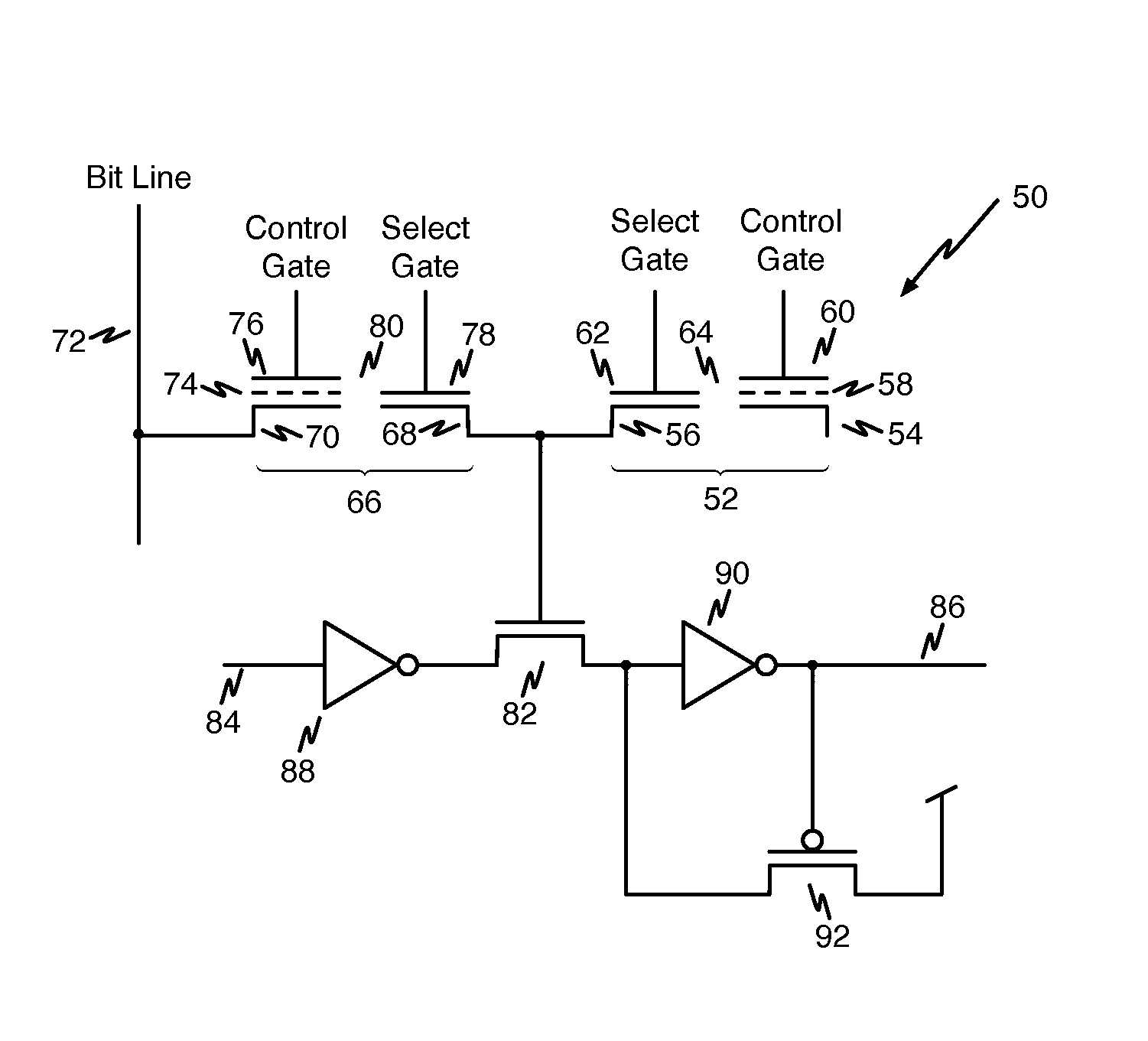
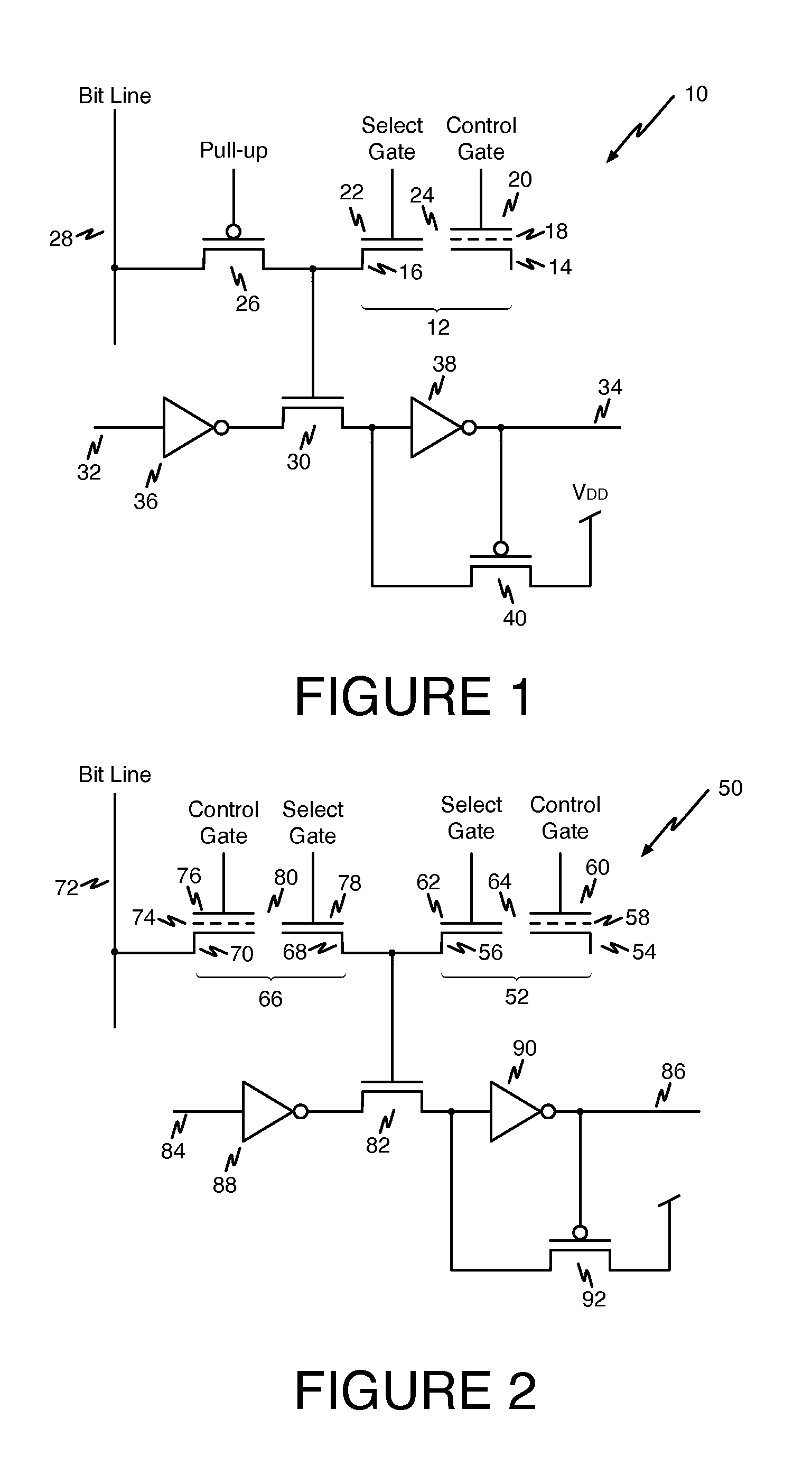
[0015]Referring first to FIG. 1, an illustrative split-gate memory cell 10 according to a first aspect of the present invention is shown. Memory cell 10 includes a split-gate non-volatile memory transistor shown at reference numeral 12. Split-gate non...


PUM


Abstract

A split-gate memory cell, includes an n-channel split-gate non-volatile memory transistor having a source, a drain, a select gate over a thin oxide, and a control gate over a non-volatile gate material and separated from the select gate by a gap. A p-channel pull-up transistor has a drain coupled to the drain of the split-gate non-volatile memory transistor, a source coupled to a bit line, and a gate. A switch transistor has first and second source/drain diffusions, and a gate coupled to the drains of the split-gate non-volatile memory transistor and the p-channel pull-up transistor. An inverter has an input coupled to the second source/drain diffusion of the switch transistor, and an output. A p-channel level-restoring transistor has a source coupled to a supply potential, a drain coupled to the first source/drain diffusion of the switch transistor and a gate coupled to the output of the inverter.

Description

BACKGROUND OF THE INVENTION[0001]1. Field of the Invention[0002]The present invention relates to memory cells and especially to memory cells employed in user-programmable integrated circuit devices such as field programmable gate array devices.[0003]2. The Prior Art[0004]Numerous prior memory cells have been proposed for controlling switching in user-programmable integrated circuits. Some prior schemes have employed n-channel nano-crystal or SONOS transistors as pull-down devices and used volatile p-channel transistors as pull-up devices. Other schemes have employed p-channel nano-crystal or SONOS transistors and used volatile re-channel transistors as pull-down devices. Still other schemes have used both re-channel and p-channel nano-crystal or SONOS transistors as pull-down and pull-up devices, respectively, to form push-pull memory cells.[0005]One example of a prior-art device is shown in United states Patent Publication No. 2005 / 0141266, now abandoned. Another such example is sh...

Claims


Application Information

Patent Timeline
Patent Type & Authority Patents(United States)
IPC IPC(8): G11C16/04
CPCG11C16/0425G11C16/0441G11C16/0475G11C16/0466G11C16/0458
Inventor SADD, MICHAELDHAOUI, FETHIWANG, GEORGEMCCOLLUM, JOHN
Owner MICROSEMI SOC
Why Eureka
Try Eureka