Programmable resistive memory unit with data and reference cells

a resistive memory unit and data reference technology, applied in static storage, digital storage, instruments, etc., can solve the problems of large cell size of electrical fuse using silicided polysilicon, difficult to achieve the effect of reducing cell size and cost, small cell size and cost reduction

Inactive Publication Date: 2015-05-05
ATTOPSEMI TECH CO LTD
View PDF206 Cites 44 Cited by
  • Summary
  • Abstract
  • Description
  • Claims
  • Application Information

AI Technical Summary

Benefits of technology

[0018]Embodiments of memory devices are disclosed herein. Certain embodiments disclosed concern programmable resistive device cells using polysilicon diodes as program selectors are disclosed. The programmable resistive devices can be fabricated using standard CMOS logic processes to reduce cell size and cost. In one embodiment, a programmable resistive device and memory can use diodes fabricated on a polysilicon as program selectors, where the P and N terminals of the diode are P+ and N+ implants on the same polysilicon. The same P+ and N+ implants are used to create sources or drains of core logic PMOS and NMOS devices, respectively. Advantageously, the same polysilicon can be used to create CMOS gates in standard CMOS logic processes. By using polysilicon diodes in standard CMOS processes, a small cell size can be achieved, without incurring any special processing or masks. Thus, costs can be reduced substantially for variously applications, such as embedded applications.

Problems solved by technology

As a result, the cell size of an electrical fuse using silicided polysilicon tends to be very large.
Though this technology can reduce the PCM cell size to only 6.8F2 (F stands for feature size), the diode requires very complicated process steps, such as Selective Epitaxial Growth (SEG), to fabricate, which would be very costly for embedded PCM applications.
The fuse elements 80, 84 in FIGS. 3(a) and 3(b) are relatively large structures which makes them unsuitable for some applications.

Method used


Image

  • Programmable resistive memory unit with data and reference cells
  • Programmable resistive memory unit with data and reference cells
  • Programmable resistive memory unit with data and reference cells

Examples


Embodiment Construction

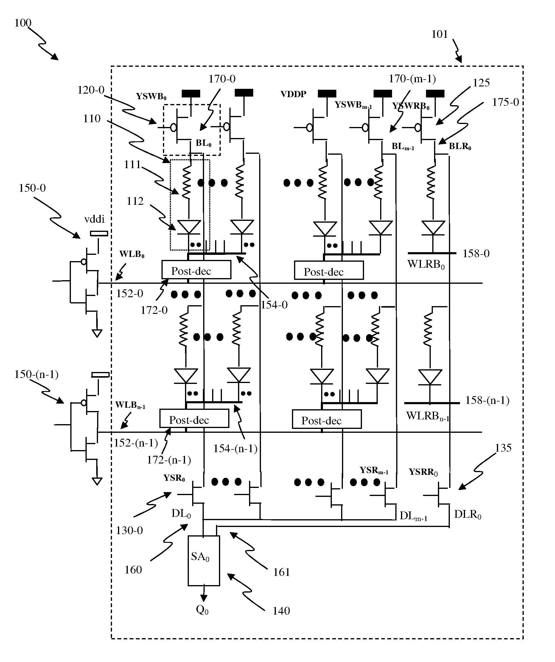
[0079]Embodiments disclosed herein use a polysilicon diode as program selector for a programmable resistive device. The diode can comprise P+ and N+ implants on a polysilicon substrate. Since the P+ and N+ implants and polysilicon are readily available in standard CMOS logic processes, these devices can be formed in an efficient and cost effective manner. There are no additional masks or process steps to save costs. The programmable resistive device can also be included within an electronic system.

[0080]Embodiments of a method and system of a programmable resistive memory having a plurality of programmable resistive memory units are disclosed. At least one of the programmable resistive memory units has at least one data cell and at least one reference cell. The data cell can have one programmable resistive element coupled to at least one diode as a program selector and also coupled to a bitline (BL). The reference cell can have a reference resistive element coupled to at least one r...


PUM


Abstract

A method and system of a programmable resistive memory having a plurality of programmable resistive memory units. At least one of the programmable resistive memory units has at least one data cell and at least one reference cell. The data cell can have one programmable resistive element coupled to at least one diode as a program selector and also coupled to a bitline (BL). The reference cell can have a reference resistive element coupled to at least one reference diode as reference program selector and also coupled to a reference bitline (BLR). In one embodiment, the reference resistive element can have substantially the same material, structure, or shape of the programmable resistive element. In one embodiment, the reference diode can have the same material, structure, or shape of the diode serving as the program selector diode.

Description

CROSS-REFERENCE TO RELATED APPLICATIONS[0001]This application is a continuation-in-part of U.S. patent application Ser. No. 13 / 026,725, filed on Feb. 14, 2011, and entitled “CIRCUIT AND SYSTEM OF USING A JUNCTION DIODE AS PROGRAM SELECTOR FOR RESISTIVE DEVICES,” which is hereby incorporated herein by reference, and which in turn claims priority benefit of (i) U.S. Provisional Patent Application No. 61 / 375,653, filed on Aug. 20, 2010 and entitled “CIRCUIT AND SYSTEM OF USING JUNCTION DIODE AS PROGRAM SELECTOR FOR RESISTIVE DEVICES IN CMOS LOGIC PROCESSES,” which is hereby incorporated herein by reference; and (ii) U.S. Provisional Patent Application No. 61 / 375,660, filed on Aug. 20, 2010 and entitled “CIRCUIT AND SYSTEM OF USING POLYSILICON DIODE AS PROGRAM SELECTOR FOR RESISTIVE DEVICES IN CMOS LOGIC PROCESSES,” which is hereby incorporated herein by reference.[0002]This application is a continuation-in-part of U.S. patent application Ser. No. 13 / 026,650, filed on Feb. 14, 2011 now ...

Claims


Application Information

Patent Timeline
Patent Type & Authority Patents(United States)
IPC IPC(8): G11C11/00G11C11/56G11C13/00G11C17/16
CPCG11C11/56G11C11/5678G11C11/5692G11C13/0002G11C13/0004G11C13/0007G11C13/0011G11C13/0023G11C13/003G11C13/0038G11C13/004G11C13/0061G11C13/0064G11C13/0069G11C17/16G11C2013/0042G11C2013/0073G11C2213/72G11C2213/74G11C19/08
Inventor CHUNG, SHINE C.
Owner ATTOPSEMI TECH CO LTD
Why Eureka
Try Eureka