Method for shielding an electronic component

a technology of electronic components and shielding methods, applied in the field of electronic components, can solve the problems of electromagnetic interference, electromagnetic interference is the generation of undesired electrical signals in electronic system circuitry, electromagnetic interference,

Inactive Publication Date: 2006-03-21
PPG IND OHIO INC
View PDF3 Cites 130 Cited by
  • Summary
  • Abstract
  • Description
  • Claims
  • Application Information

AI Technical Summary

Problems solved by technology

Electrical signals cause circuit components to radiate a portion of the spectral energy of the propagating signal causing electromagnetic interference.
Electromagnetic interference is the generation of undesired electrical signals in electronic system circuitry because of the unintentional coupling of impinging electromagnetic field energy.
Integrated circuits which have output drivers that create pulses with high amounts of spectral energy are more likely than low power drivers to cause electromagnetic interference because of a mismatch between the driver and the line impedance, and the resistance to instantaneous signal propagation imposed by the parasitics of the conductor.
These disturbances in the electromagnetic field result in reflections of the signal energy at the points where the variation occurred.
Magnetic fields possessing high intensity can induce spurious current flow in other system components.
Noise radiated from within a system can interfere with system performance by coupling with other system elements, not just adjacent conductor nets, as another form of within system electromagnetic interference.
The increasing operating frequency in these electrical systems results in increasing high frequency electromagnetic interference.
The effect of all these sources of noise is to degrade the performance or to induce errors in the systems.
The prevalence of high frequency systems and portable electronics is creating a very complex spectral environment for the operation of sensitive electrical systems.
Disadvantages of metal housings are that they are often expensive, heavy, and difficult to make in complex shapes.
The inside of a molded plastic housing may be coated with a thin metal film through vacuum metalization but this process often yields a brittle less flexible shield.
In addition, a break in the shield may require that the entire electroninc device, or significant parts of it, be discarded as waste at a considerable expense.
Conventional metalizing methods such as using conductive metal-bearing paints, vacuum plating of aluminum, physical vapor deposition of aluminum or other metals, plating on plastics, laminated metalizing methods, and using woven and coated fibers generally fail due to limited ductility, flexibility, and thermoformability.

Method used


Image

  • Method for shielding an electronic component
  • Method for shielding an electronic component
  • Method for shielding an electronic component

Examples


Embodiment Construction

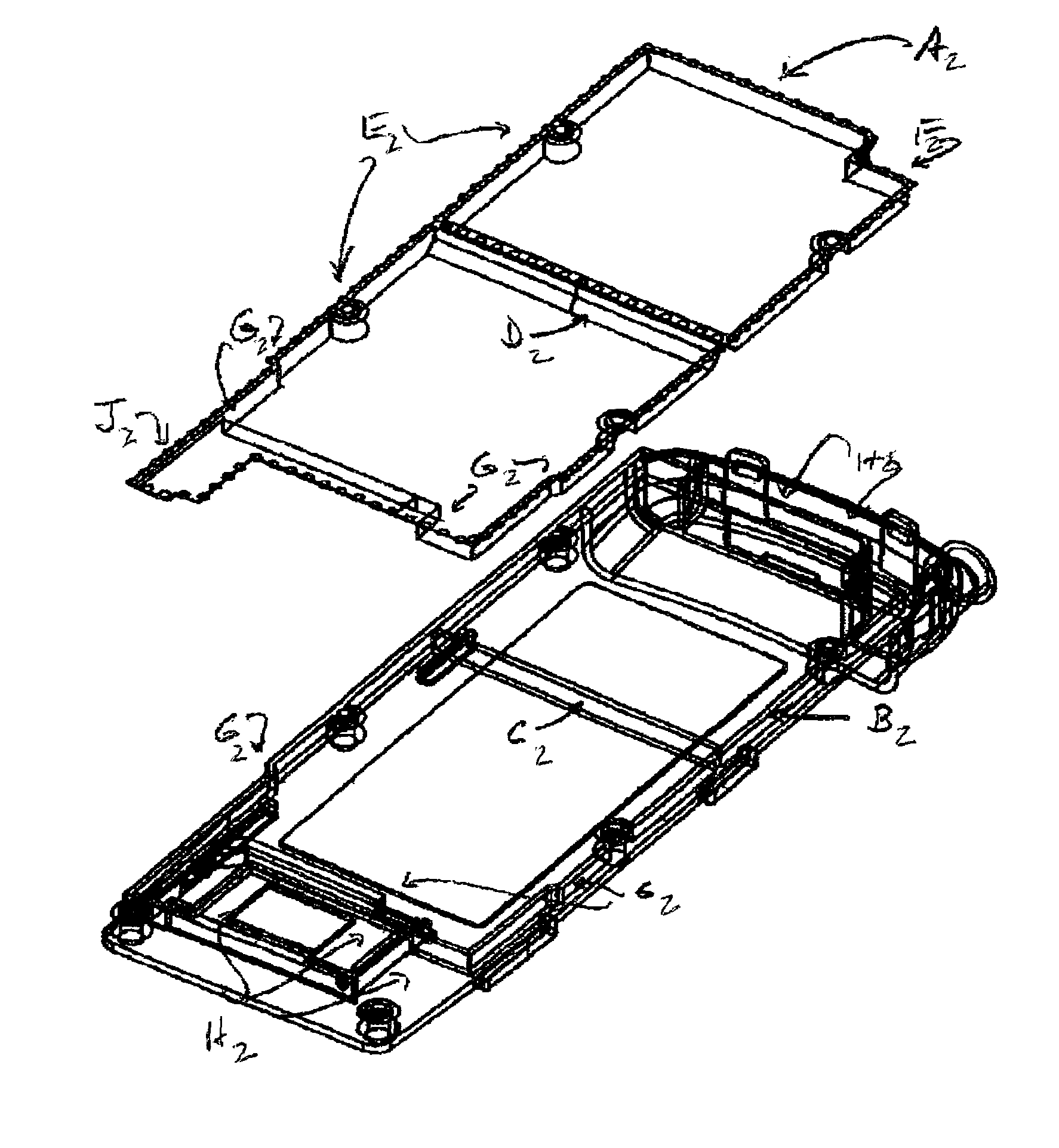
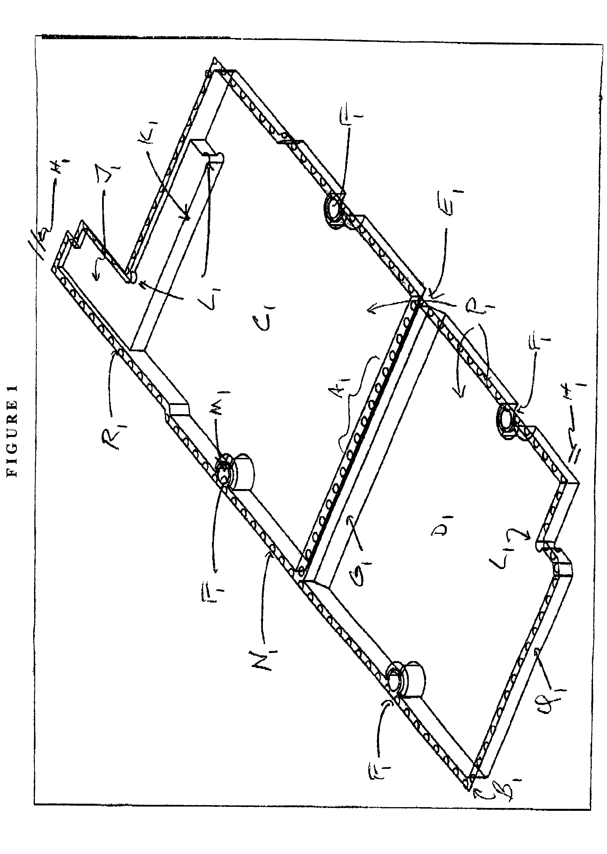
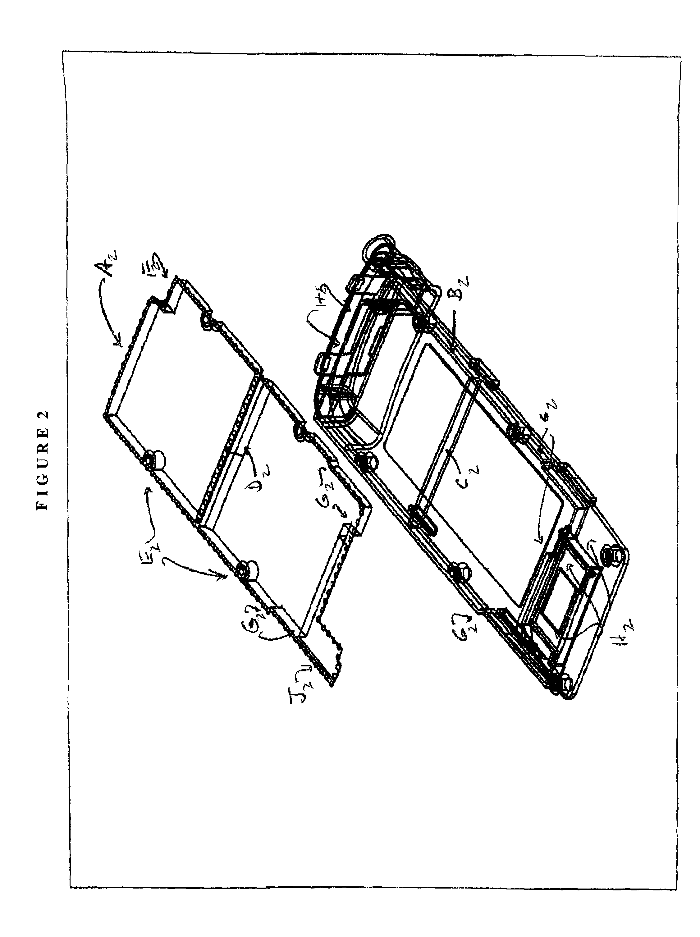
[0044]The present invention is directed to electronic components shielded from electromagnetic interference through the use of conforming shield enclosures. Conforming shield enclosures are flexible metalized thermoformed thin-wall polycarbonate polymer film substrates used to shield a radiation source. The present invention relates to conforming shielded forms for electronic component assemblies and specifically to electronic component assemblies which are shielded to protect against electromagnetic interference. Specifically, the shielded electronic component assembly comprises (a) a semiconductor device to be shielded from electromagnetic frequencies; (b) a reference potential source; (c) a housing enclosing the semiconductor device within the assembly; and (d) a conforming shield enclosure electrically connected to the reference potential source, wherein the conforming shield enclosure comprises a metalized thermoformable polymer having dimensions conforming to the inside of the...


PUM

PropertyMeasurementUnit
thicknessaaaaaaaaaa
thicknessaaaaaaaaaa
frequencyaaaaaaaaaa

Abstract

The present invention is directed to electronic components shielded from electromagnetic interference through the use of conforming shield enclosures. Conforming shield enclosures are flexible metalized thermoformed thin-wall polycarbonate polymer film substrates used to shield a radiation source. The present invention relates to conforming shielded forms for electronic component assemblies and specifically to electronic component assemblies which are shielded to protect against electromagnetic and radiofrequency interference. Specifically, the shielded electronic component assembly comprises (a) a semiconductor device to be shielded from electromagnetic frequencies; (b) a reference potential source; (c) a housing enclosing the semiconductor device within the assembly; and (d) a conforming shield enclosure electrically connected to the reference potential source. The conforming shield enclosure comprises a flexible, metalized thermoformable polymer having dimensions conforming to the inside of the housing and enclosing and thereby shielding the semiconductor device from electromagnetic frequencies. The conforming shield enclosure is prepared by paint metalization.

Description

[0001]This application is a divisional application of parent application Ser. No. 09 / 531 / 745, filed Mar. 21, 2000 now U.S. Pat. No. 6,483,719.FIELD OF THE INVENTION[0002]The present invention is directed to electronic components shielded from electromagnetic interference through the use of conforming shield enclosures. Conforming shield enclosures are flexible metalized thermoformed thin-wall polycarbonate polymer film substrates used to shield a radiation source. The present invention relates to conforming shielded forms for electronic component assemblies and specifically to electronic component assemblies which are shielded to protect against electromagnetic and radio frequency interference. Specifically, the shielded electronic component assembly comprises (a) a semiconductor device to be shielded from electromagnetic frequencies; (b) a reference potential source; (c) a housing enclosing the semiconductor device within the assembly; and (d) a conforming shield enclosure electric...

Claims


Application Information

Patent Timeline
Patent Type & Authority Patents(United States)
IPC IPC(8): H05K3/30C08J7/06H05K9/00
CPCH05K9/003Y10T29/49002Y10T29/49171Y10T29/49144Y10T29/49146Y10T29/49988Y10T29/4913H05K9/0029H05K9/00H05K3/30H05K3/34
Inventor BACHMAN, BRUCE
Owner PPG IND OHIO INC
Why Eureka
Try Eureka