
Semiconductor wafer holder and electroplating system for plating a semiconductor wafer

a technology of semiconductor wafers and electroplating systems, which is applied in the direction of electrical-based machining electrodes, coatings, manufacturing tools, etc., can solve the problems of cumbersome approach, conductive pins cannot be reliably contacted with the conductive layer of semiconductor wafers, and it is not easy to mount semiconductor wafers to the holder

Inactive Publication Date: 2006-04-04
EBARA CORP
View PDF7 Cites 46 Cited by
  • Summary
  • Abstract
  • Description
  • Claims
  • Application Information

AI Technical Summary

Benefits of technology

[0028]The locking member is engaged with the lockable portion so as to lock the first and second holding members together when the clamping ring is held in the clamp position.
[0029]Also, the first holding mem

Problems solved by technology

With such an arrangement, however, it is not easy to mount the semiconductor wafer to the holder.
Also, the conductive pin can not be reliably contacted with the conductive layer of the semiconductor wafer.
Such an approach is, however, cumbersome.
It is also difficult to apply uniform torque to each bolt.
Uneven application of torque may cause the electrolytic solution to reach the conductive pin.

Method used


Image

  • Semiconductor wafer holder and electroplating system for plating a semiconductor wafer
  • Semiconductor wafer holder and electroplating system for plating a semiconductor wafer
  • Semiconductor wafer holder and electroplating system for plating a semiconductor wafer

Examples


Embodiment Construction

[0050]The present invention will now be described with reference to the drawings. FIGS. 1, 2, 3A and 3B show a semiconductor wafer holder according to one embodiment of the present invention. FIGS. 7A, 7B, 8, 9 and 10 show another embodiment of the semiconductor wafer holder according to the present invention.

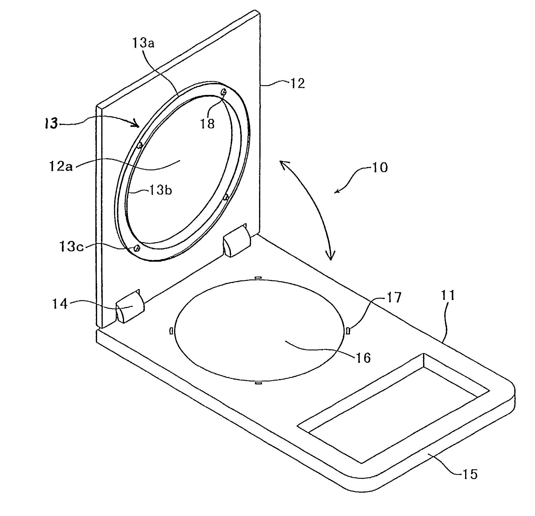
[0051]FIG. 1 is a perspective view showing the outer appearance of a semiconductor wafer holder according to one embodiment of the present invention. As shown, a holder 10 includes a first, plate-like holding member 11 made of an electrically insulative material (such as synthetic resin), and a second, plate-like holding member 12 made of an electrically insulative material (such as synthetic resin) and provided with an annular seal or packing 13. The second holding member 12 is connected to the first holding member 11 by means of a hinge mechanism 14. A handle 15 is formed at one end of the first holding member 11 remote from the hinge mechanism 14.

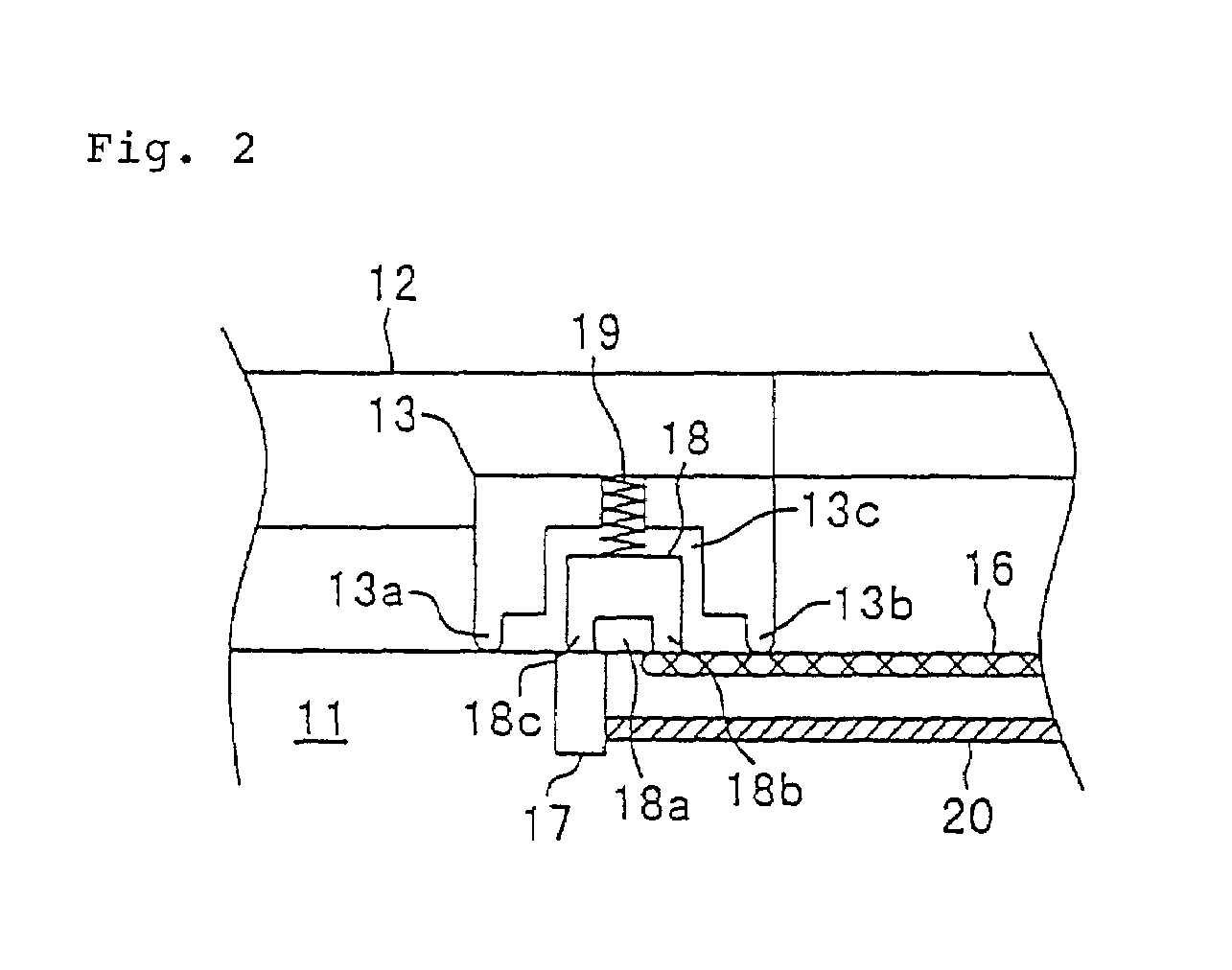
[0052]A recess is formed in ...


PUM

PropertyMeasurementUnit
Electrical conductoraaaaaaaaaa

Abstract

A semiconductor wafer holder including first and second holding members between which a semiconductor wafer is held. The second holding member includes a second conductive element placed in contact with a first conductive element of the first holding member and the semiconductor wafer. A ring clamp is used to press the second holding member against the first holding member for holding of the semiconductor wafer.

Description

[0001]This is a continuation application of Ser. No. 09 / 463,698, filed Jan. 31, 2000 now abandoned, which application is a 371 of PCT / JP 99 / 02576 filed on May 18, 1999.BACKGROUND OF THE INVENTION[0002]1. Technical Field[0003]The present invention relates to a semiconductor wafer holder and an electroplating system for plating a semiconductor wafer. The semiconductor wafer holder is designed to hold a semiconductor wafer during electrolytic plating.[0004]2. Description of Related Art[0005]A conventional semiconductor wafer holder holds a semiconductor wafer so that a conductive pin is placed in contact with a conductive layer of the semiconductor wafer during electrolytic plating. The wafer holder together with the semiconductor wafer is immersed in an electrolyte bath within which an electrolytic solution is contained. Electrical current is supplied to the semiconductor wafer through the electrolytic solution and the conductive pin for electrolytic plating of the semiconductor wafer...

Claims


Application Information

Patent Timeline
IPC IPC(8): C25D17/00C25D7/12H01L21/687
CPCC25D17/06C25D17/001H01L21/68721
Inventor YOSHIOKA, JUNICHIROMUKAIYAMA, YOSHITAKA
Owner EBARA CORP
Features
  • Generate Ideas
  • Intellectual Property
  • Life Sciences
  • Materials
  • Tech Scout
  • Unparalleled Data Quality
  • Higher Quality Content
  • 60% Fewer Hallucinations
Learn More