Microprocessor on-chip testing architecture and implementation

a microprocessor and test architecture technology, applied in the field of on-chip test circuitry, can solve the problems of large power consumption of lbist testing, limited test coverage, and error in tested logi

Inactive Publication Date: 2006-04-11
INTEL CORP
View PDF5 Cites 17 Cited by
  • Summary
  • Abstract
  • Description
  • Claims
  • Application Information

AI Technical Summary

Problems solved by technology

If there is a difference between the actual output data and the expected output data, then there is an error in the tested logic.
There are several problems, however, with the JTAG systems that are present in the art.
First, test data generation and diagnostics are done off-chip, which can lead to limited test coverage due to test data volume and/or excessiv

Method used


Image

  • Microprocessor on-chip testing architecture and implementation
  • Microprocessor on-chip testing architecture and implementation
  • Microprocessor on-chip testing architecture and implementation

Examples


Embodiment Construction

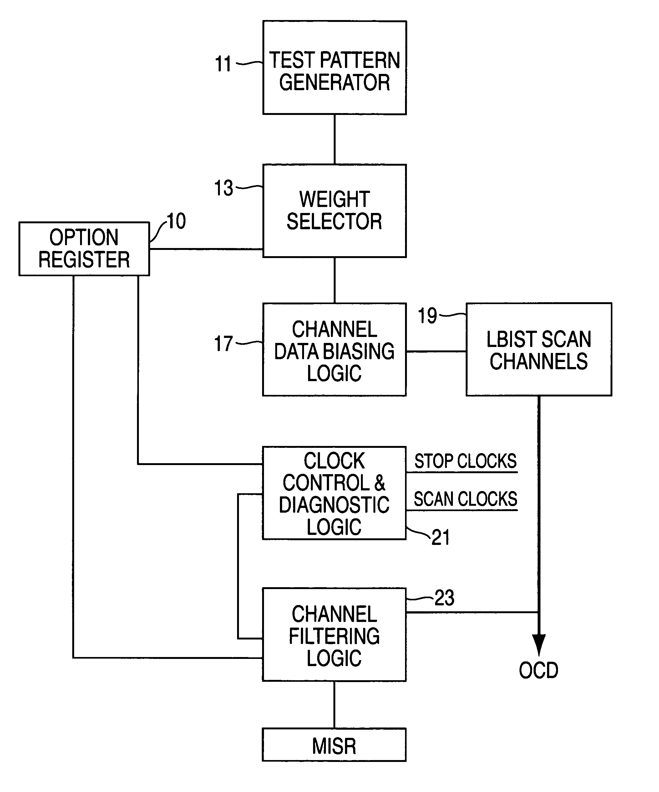
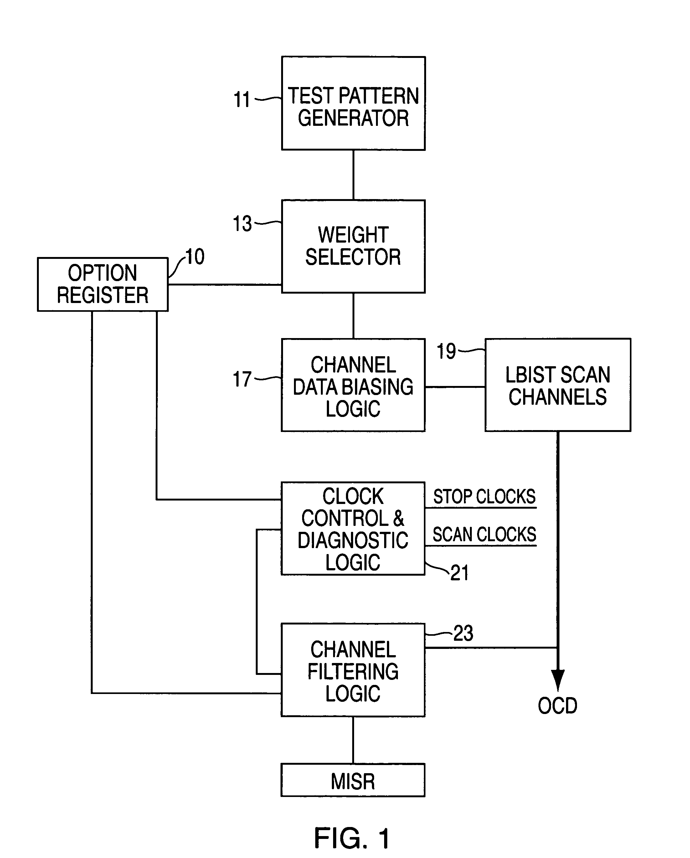
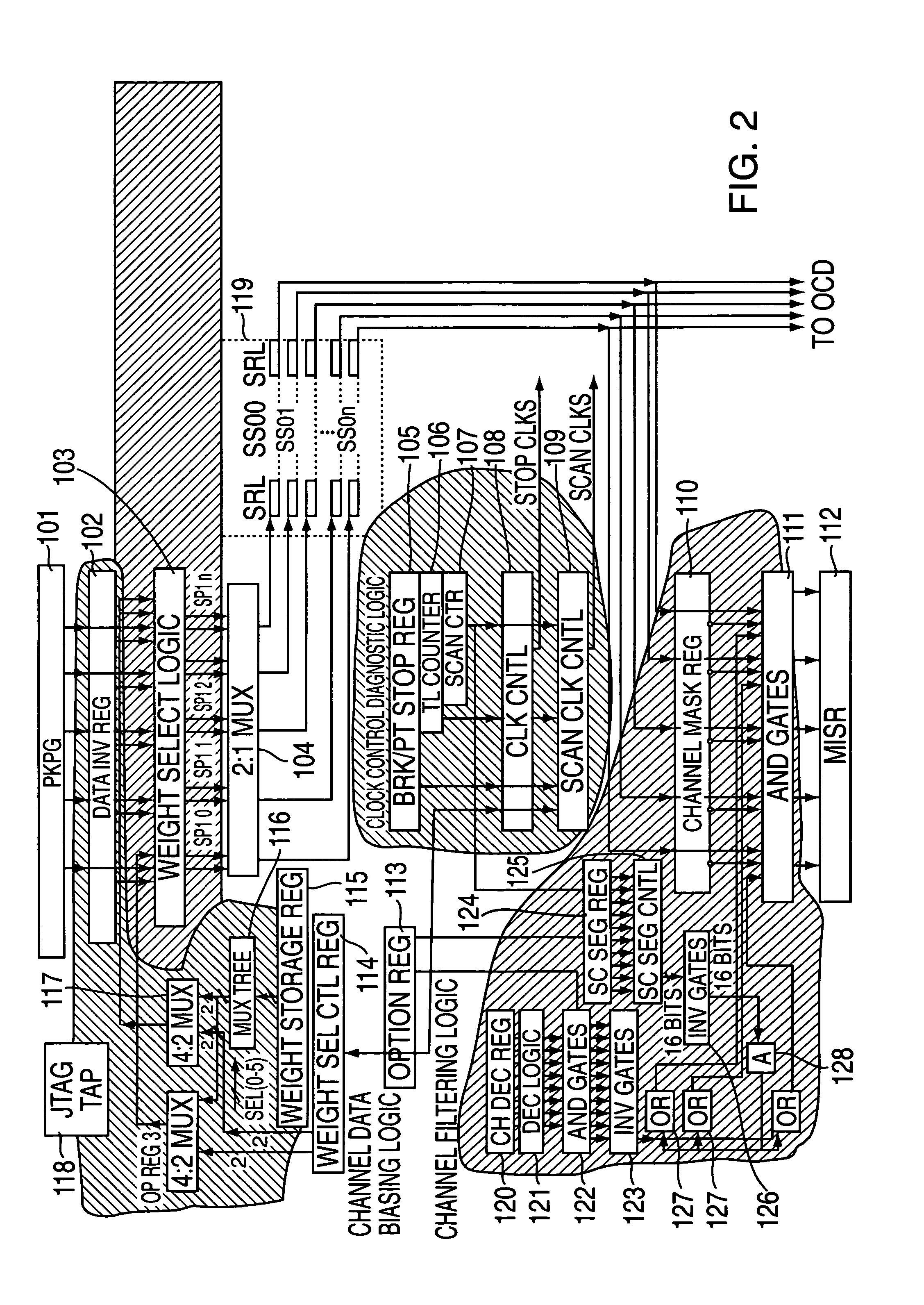
[0009]Referring to FIG. 1, a general block diagram of an LBIST architecture is shown constructed according to an embodiment of the present invention. A pattern generator 11 provides raw data to be input into test circuitry on the chip. A weight selector 13 is coupled to pattern generator 11 to provide a particular weighting of the raw data based on the value in option register 10. The output of the weight selector is supplied to channel data biasing logic 17, which, in turn supplies the data to the LBIST scan channels 19 (e.g., such as those that are known in the art). Clock control & diagnostic logic 21 generates stop and scan clocks for the LBIST scan channels. The scan clocks are a pair of clocking signals supplied to each scan chain element and are used to move data between the LBIST scan channels by controlling the latches or flip-flops present in these elements. A third clock may be used as a functional clock (i.e., one that is used by the logic that is being tested in the LBI...


PUM


Abstract

A method and apparatus are presented for on-chip testing of circuits in testing channels. In an embodiment of the present invention, the system includes a weight selector that allows for a wide variety of weighting of test data that is to be supplied to the testing channels. For example, the weight selector may be used to weight all bits in all channels or individual bits in a particular channel. Clock control and diagnostic logic may also be provided to selectively supply scan, functional, and/or stop clock signals to the testing channels. Channel filtering logic may be also provided to mask output data from a selected testing channel as desired. The method and apparatus may provide improved testing performance and power savings.

Description

BACKGROUND OF THE INVENTION[0001]The present invention pertains to on-chip test circuitry. More particularly, the present invention pertains to a logical built-in self test (LBIST) circuit for selectively testing channels in a microprocessor or other complex semiconductor circuitry.[0002]There are numerous on-chip test circuitry schemes available in the art. For example, the IEEE 1149.1 (Joint Test Action Group (JTAG) 1990), provides an on-chip testing system that includes a scan chain. The scan chain includes a plurality of elements, where each element includes a flip-flop or latch. During initialization, a first set of input data is provided to the first flip-flop of each of the test channels. A scan clock is used to move this data from the first flip-flop into the test channel. At the same time, the next set of input data is provided to the first flip-flops. Each scan chain element is coupled to a subset of logic on the chip to be tested (i.e., the test channel). The initializati...

Claims


Application Information

Patent Timeline
IPC IPC(8): G01R31/28G01R31/3181G06F11/263
CPCG06F11/263G01R31/31813
Inventor JABER, TALAL K.
Owner INTEL CORP
Why Eureka
Try Eureka