Surface passivation of GaN devices in epitaxial growth chamber

a gallium nitride and growth chamber technology, applied in the direction of semiconductor devices, basic electric elements, electrical apparatus, etc., can solve the problems of reducing the effectiveness and reproducibility of the ex-situ passivation process, affecting and affecting the performance of electronic devices. , to achieve the effect of reducing the degradation of the operation of the hem

Inactive Publication Date: 2006-05-30
QORVO US INC
View PDF18 Cites 65 Cited by
  • Summary
  • Abstract
  • Description
  • Claims
  • Application Information

AI Technical Summary

Benefits of technology

[0006]The GaN structure including the PSN passivation layer may be used to fabricate electrical devices such as a high electron mobility transistor (HEMT) or a metal-insulator-semiconductor field effect transistor (MISFET). For the HEMT, the structural epitaxial layers include a transitional layer, a GaN buffer layer, and an aluminum gallium nitride (AlGaN) Schottky layer. Optionally, the structural epitaxial layers may include a sub-buffer layer between the transitional layer and the GaN buffer layer and / or a GaN termination layer deposited on the AlGaN Schottky layer. The PSN passivation layer is etched in order to form source, gate, and drain contacts. The PSN passivation layer serves to essentially eliminate degradation of the operation of the HEMT due to phenomena such as radio frequency (RF) dispersion and current collapse by passivating the surface traps on the surface of the Schottky layer or the optional GaN termination layer. In a similar fashion, the MISFET may be fabricated from the GaN structure including the PSN passivation layer by forming the gate contact on the PSN passivation layer.

Problems solved by technology

Epitaxial growth of GaN structures leads to phenomena associated with surface traps, which degrade performance of electronic devices, on the surface of the GaN structure.
The reactions associated with surface traps degrade the performance of electronic devices fabricated using the GaN structure by causing radio frequency (RF) dispersion and current collapse.
By exposing the GaN structure to the atmosphere, oxidation may occur on the surface of the GaN structure, thereby decreasing the effectiveness and reproducibility of the ex-situ passivation process.

Method used


Image

  • Surface passivation of GaN devices in epitaxial growth chamber
  • Surface passivation of GaN devices in epitaxial growth chamber
  • Surface passivation of GaN devices in epitaxial growth chamber

Examples


Embodiment Construction

[0012]The embodiments set forth below represent the necessary information to enable those skilled in the art to practice the invention and illustrate the best mode of practicing the invention. Upon reading the following description in light of the accompanying drawing figures, those skilled in the art will understand the concepts of the invention and will recognize applications of these concepts not particularly addressed herein. It should be understood that these concepts and applications fall within the scope of the disclosure and the accompanying claims.

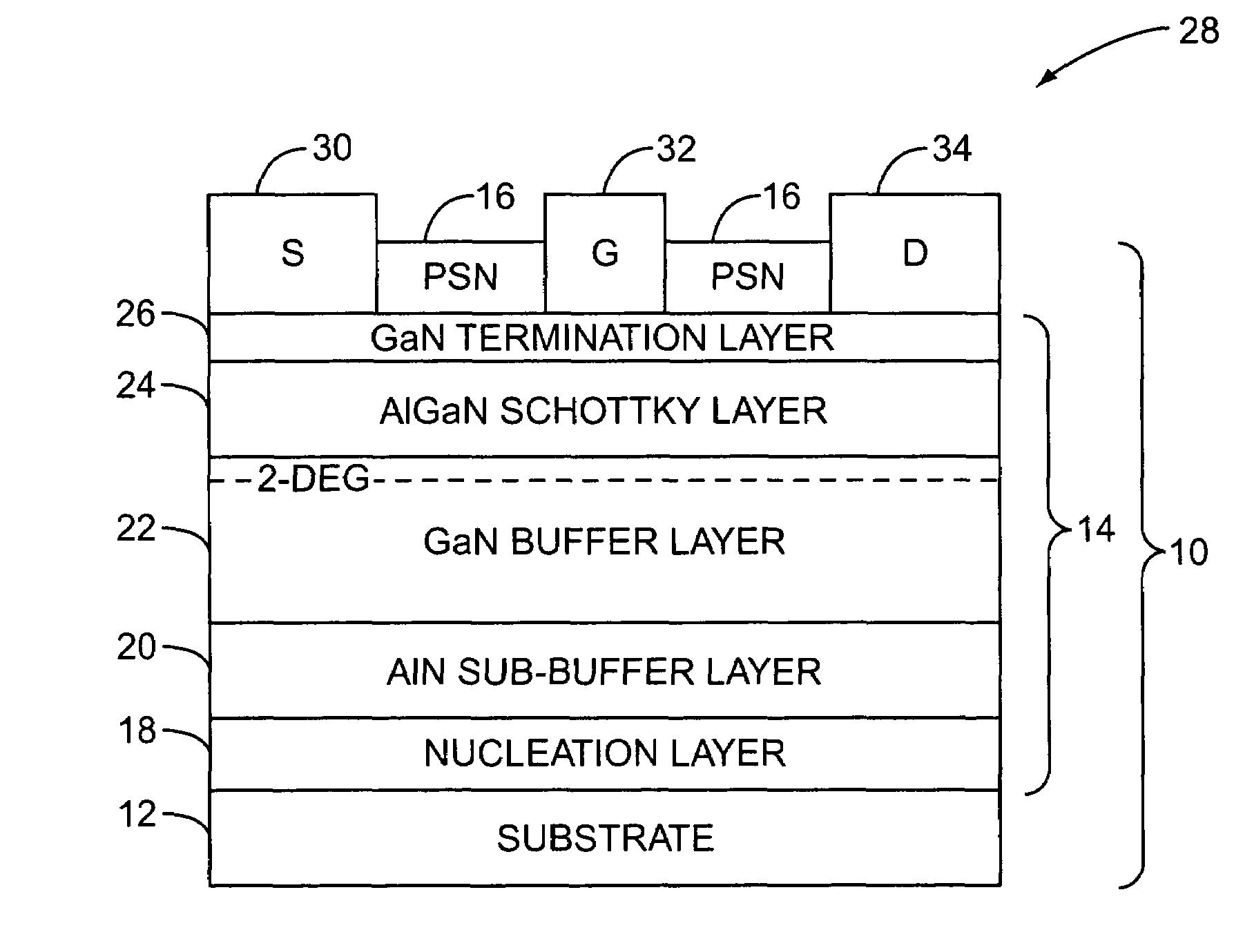
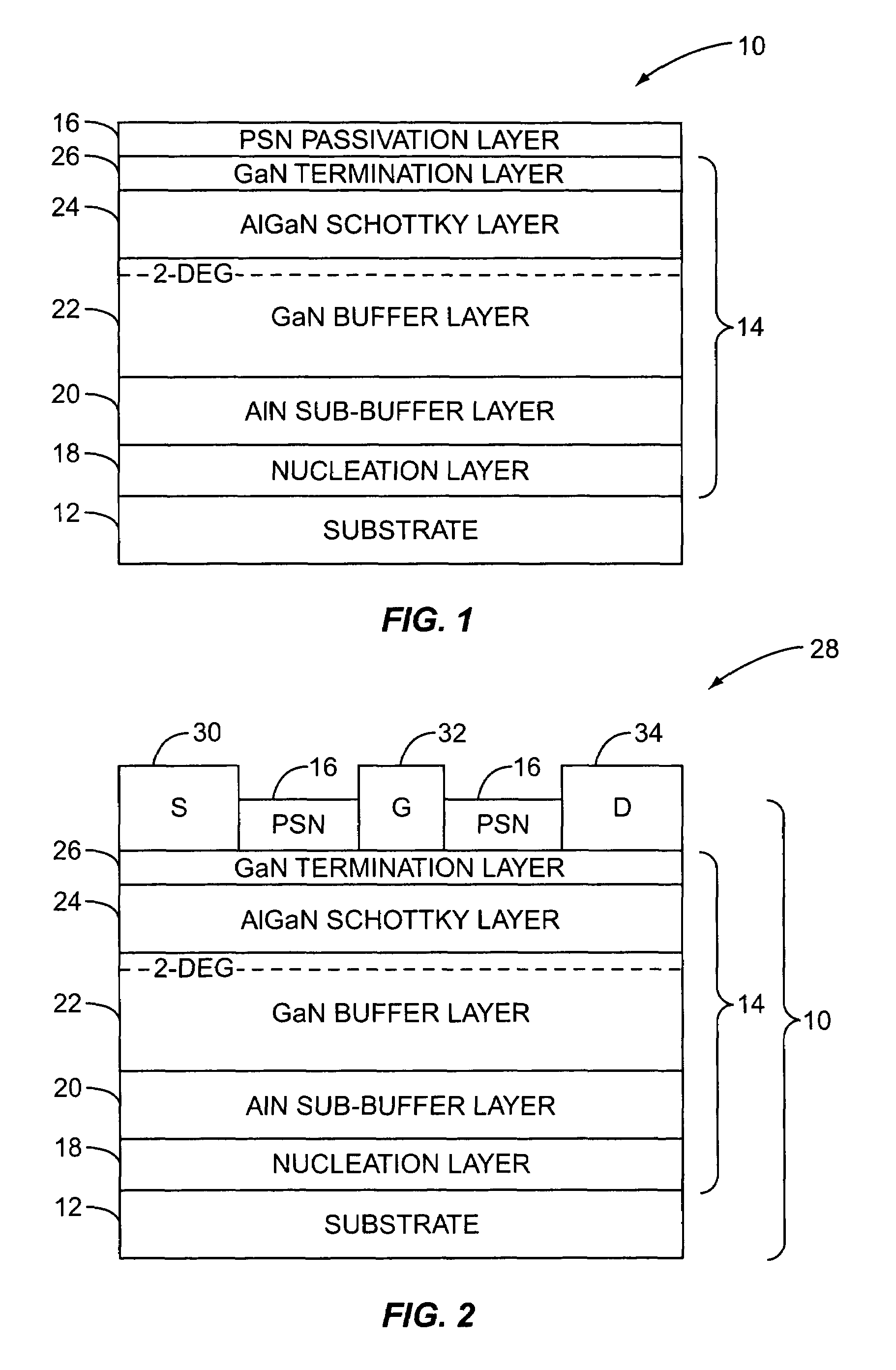
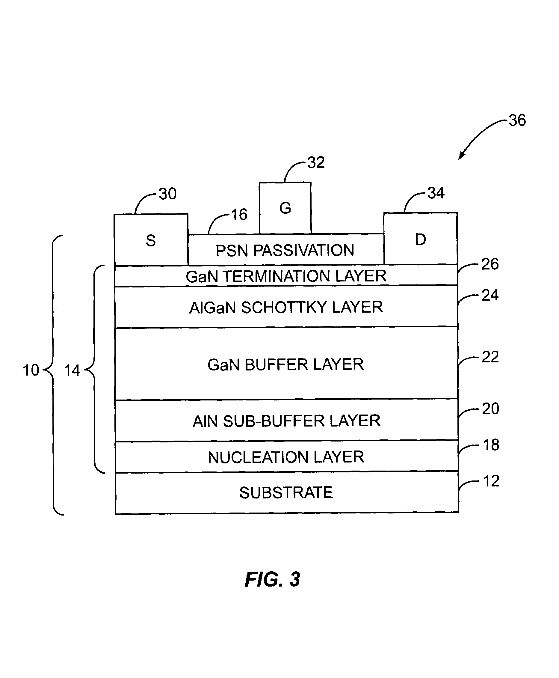
[0013]FIG. 1 illustrates a gallium nitride (GaN) structure having been passivated before removal from a growth chamber (not shown) according to the present invention. The GaN structure 10 includes a substrate 12, structural epitaxial layers 14, and a (pyrolitic silicon nitride) PSN passivation layer 16. In one embodiment, the PSN passivation layer 16 is a thermally assisted silicon nitride passivation layer. The PSN passivation la...


PUM

PropertyMeasurementUnit
thickaaaaaaaaaa
source-drain breakdown voltageaaaaaaaaaa

Abstract

The present invention relates to passivation of a gallium nitride (GaN) structure before the GaN structure is removed from an epitaxial growth chamber. The GaN structure includes one or more structural epitaxial layers deposited on a substrate, and the passivation layer deposited on the structural epitaxial layers. In general, the passivation layer is a dielectric material deposited on the GaN structure that serves to passivate surface traps on the surface of the structural epitaxial layers. Preferably, the passivation layer is a dense, thermally deposited silicon nitride passivation layer.

Description

[0001]This application claims the benefit of provisional patent application Ser. No. 60 / 503,917, filed Sep. 19, 2003, the disclosure of which is hereby incorporated by reference in its entirety.FIELD OF THE INVENTION[0002]The present invention relates to surface passivation of a gallium nitride (GaN) epitaxial structures, and more particularly relates to thermally assisted deposition of silicon nitride passivation of the GaN structures while in a GaN growth chamber.BACKGROUND OF THE INVENTION[0003]Gallium nitride (GaN) offers substantial opportunity to enhance performance of electronic devices such as high electron mobility transistors (HEMTs) and metal-insulator-semiconductor field effect transistors (MISFETs). Epitaxial growth of GaN structures leads to phenomena associated with surface traps, which degrade performance of electronic devices, on the surface of the GaN structure. The surface traps are open bonding sites, on the surface of the GaN structure caused by an abrupt termin...

Claims


Application Information

Patent Timeline
Patent Type & Authority Patents(United States)
IPC IPC(8): H01L21/84H01L21/338H01L31/0328
CPCH01L29/7787H01L29/66462H01L21/3185H01L29/2003H01L21/0217H01L21/02271
Inventor SMART, JOSEPHGRIDER, DAVIDGIBB, SHAWNHOSSE, BROOKSHEALY, JEFFREY
Owner QORVO US INC
Why Eureka
Try Eureka