Stacked microelectronic assemblies with central contacts

a technology of microelectronic assemblies and central contacts, which is applied in the direction of semiconductor devices, semiconductor/solid-state device details, electrical apparatus, etc., can solve the problems of cost and reliability problems, and the approach offers only limited reduction of the aggregate area of the circuit panel occupied

Active Publication Date: 2006-06-13
TESSERA INC
View PDF2 Cites 103 Cited by
  • Summary
  • Abstract
  • Description
  • Claims
  • Application Information

AI Technical Summary

Problems solved by technology

However, this approach suffers from cost and reliability problems.
This approach offers only limited reduction in the aggregate area of the circuit panel occupied by the chips.

Method used


Image

  • Stacked microelectronic assemblies with central contacts
  • Stacked microelectronic assemblies with central contacts
  • Stacked microelectronic assemblies with central contacts

Examples


first embodiment

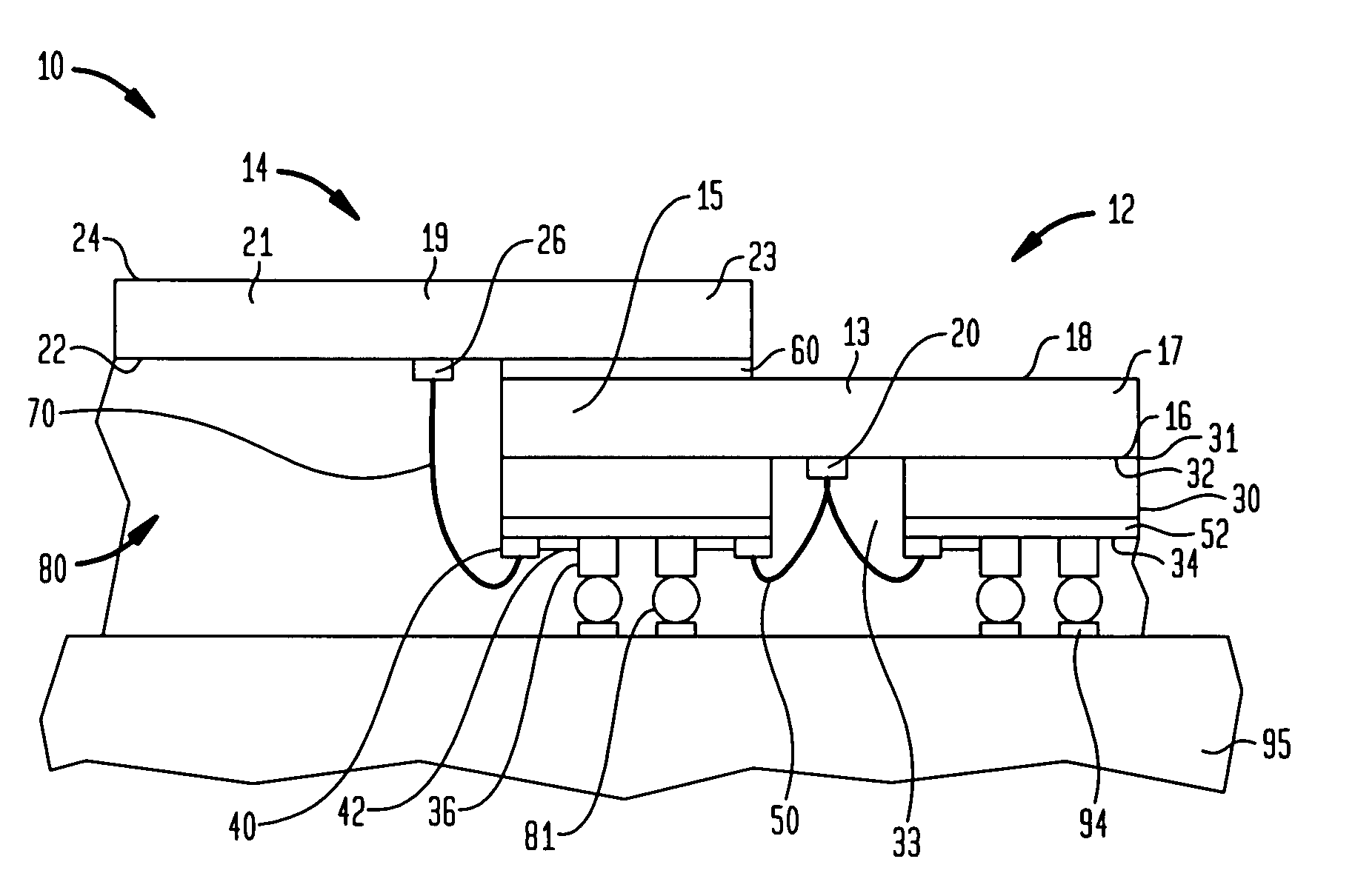
[0020]Contacts 20 on the first microelectronic element 12 are exposed within central region 13 of front surface 16. For example, contacts 20 may be formed as one or two parallel rows adjacent to the center of surface 16. Microelectronic element 14 is arranged similarly to microelectronic element 12, in that it has a front surface 22, a back surface 24 opposite the front surface and electrical contacts 26 are exposed on the front surface 22. Microelectronic element 14 also includes a central region 19 and first and second end regions 21 and 23 adjacent to central region 19. In the invention, as shown in FIG. 1, each microelectronic element 12 and 14 is a conventional semiconductor chip. Similarly, contacts 26 of second microelectronic element 14 are disposed within central region 19 of front surface 22 and may also be formed as one or two parallel rows adjacent the center of front surface 22.

[0021]The front surface 16 of the first microelectronic element faces downwardly. Second micr...

third embodiment

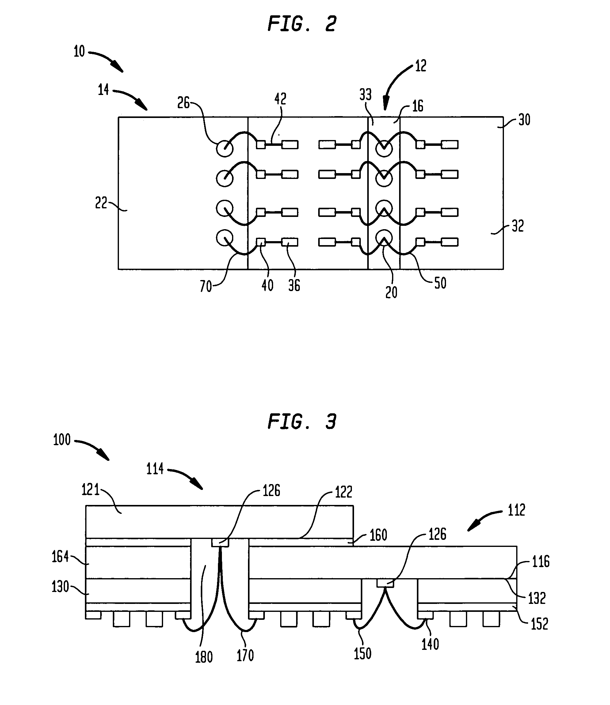
[0038]As shown in FIG. 5, the invention makes use of the A-B-A configuration by continuing the structure horizontally outwards. FIG. 5 is a skeletal depiction of a B-A-B-A-B configuration. The structure may have a configuration of A-B-A-B-A or A-B-A-B or B-A-B-A-B, or any other combination of the two where a structure A and a structure B are adjacent to one another. These structures could be extended out indefinitely until a required amount of microelectronics elements are met. Additionally, structures that follow varying designs such as having a plurality of A structures adjacent to one another without an overlying B structure may be employed.

[0039]In an alternate embodiment of the present invention as shown in FIG. 6, assembly 300 includes microelectronic elements denoted by the structure A altered so as to include a substantially continuous dielectric element 330 underlying at least one microelectronic element denoted A. For this discussion microelectronic element 312 will repres...


PUM


Abstract

A stacked microelectronic assembly includes a dielectric element and a first and second microelectronic element stacked one on top of the other with the first microelectronic element underlying at least a portion of the second microelectronic element. The first microelectronic element and the second microelectronic element have front surfaces on which exposed on a central region of the front surface are contacts. A spacer layer may be provided under a portion of the second microelectronic element opposite a portion of the second microelectronic element overlying the first microelectronic element. Additionally, a third microelectronic element may be substituted in for the spacer layer so that the first microelectronic element and the third microelectronic element are underlying opposing sides of the second microelectronic element.

Description

CROSS REFERENCE TO RELATED APPLICATIONS[0001]This application claims the benefit of the filing date of U.S. Provisional Patent Application No. 60 / 519,130 filed Nov. 12, 2003, the disclosure of which is hereby incorporated herein by reference.BACKGROUND OF THE INVENTION[0002]The present invention relates to stacked microelectronic assemblies and methods of making such assemblies, to methods of forming such assemblies and to components useful in such assemblies.[0003]Semiconductor chips are commonly provided as individual, prepackaged units. A standard chip has a flat, rectangular body with a large front face having contacts connected to the internal circuitry of the chip. Each individual chip typically is mounted in a package which, in turn, is mounted on a circuit panel such as a printed circuit board and which connects the contacts of the chip to conductors of the circuit panel. In many conventional designs, the chip package occupies an area of the circuit panel considerably larger...

Claims


Application Information

Patent Timeline
Patent Type & Authority Patents(United States)
IPC IPC(8): H01L23/48H01L25/065
CPCH01L25/0652H01L2224/4824H01L2225/06562H01L2924/15311H01L2224/06136H01L2924/01322H01L2224/32145H01L2224/32225H01L2924/01087H01L23/48
Inventor HABA, BELGACEM
Owner TESSERA INC
Why Eureka
Try Eureka