Image signal processing device for minimizing false signals at color boundaries

Inactive Publication Date: 2006-08-22
FUJIFILM CORP
View PDF29 Cites 4 Cited by
  • Summary
  • Abstract
  • Description
  • Claims
  • Application Information

AI Technical Summary

Benefits of technology

[0010]It is therefore an object of the present invention to provide an image signal processing device capable of gen

Problems solved by technology

However, the conventional device of the type determining the component of the luminance signal lying in a high frequency range by using two color component signals on two adjoining scanning lines has some p

Method used


Image

  • Image signal processing device for minimizing false signals at color boundaries
  • Image signal processing device for minimizing false signals at color boundaries
  • Image signal processing device for minimizing false signals at color boundaries

Examples


Embodiment Construction

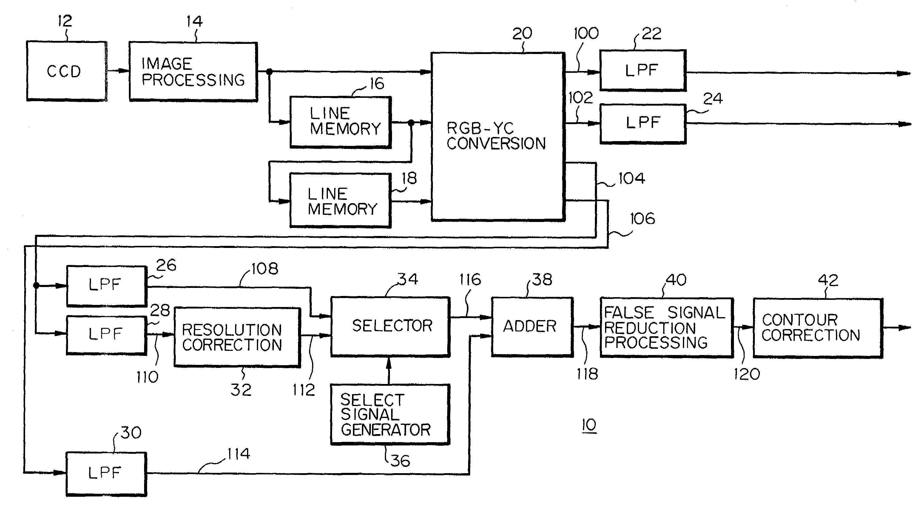
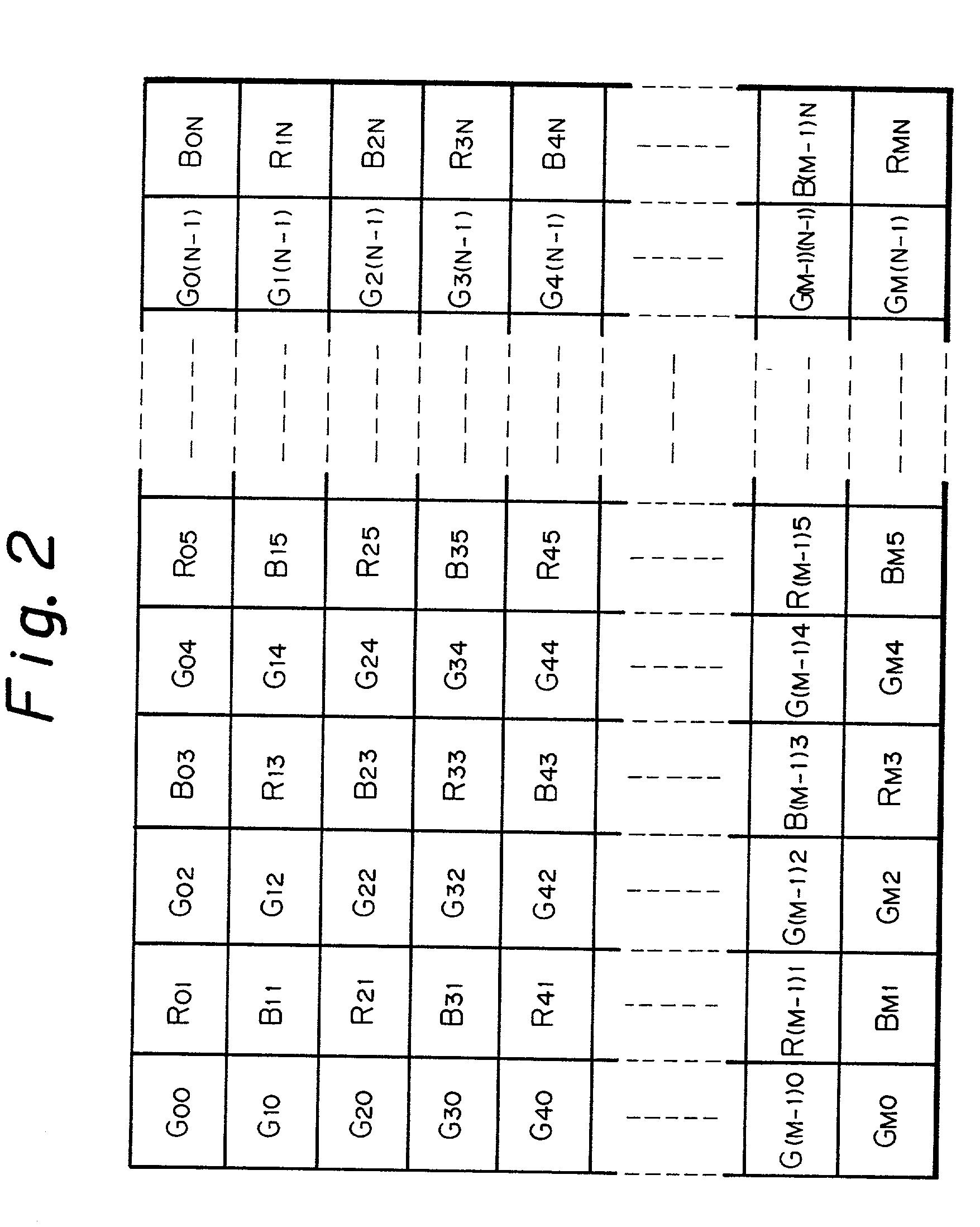
[0038]Referring to FIG. 1 of the drawings, an image signal processing device embodying the present invention is shown and generally designated by the reference numeral 10. As shown, the image signal processing device 10 includes a CCD image sensor or solid state imaging device 12. The image sensor 12 includes a bidimensional light-sensitive portion having several ten thousand to several hundred thousand pixels. A G stripe, R / B full checker color filter is fitted on the image sensor 12. In a specific configuration of the color filter, R, G and B filter components transmitting R, G and B color components, respectively, are arranged in a repetitive GRGB pattern on odd lines and arranged in a repetitive GBGR pattern on even lines. In this configuration, the G filter components extend vertically in the form of stripes while the R and B filter components form a checker pattern. Each of R, G and B color filter components corresponds to a single pixel.

[0039]When an optical image is focused ...


PUM


Abstract

An image signal processing device of the present invention includes an RGB-YC conversion for converting color component signals output from a CCD (Charge Coupled Device) image sensor to luminance signals and components thereof lying in a high frequency range. The luminance signals and their components lying in a high frequency range are fed to a first, a second and a third low pass filter (LPF), respectively. Luminance signals output from a third LPF are fed to an adder while components lying in a high frequency range are fed from the first LPF to a selector. Further, the components output from the second LPF are fed to the selector via a resolution correcting section. The selector selects either one of the two different kinds of components input thereto. The adder adds the luminance signals output from the third LPF and the components selected by the selector and thereby outputs second luminance signals. A false signal reducing section reduces false signals contained in the second luminance signals and appearing at horizontal color boundaries and feeds the resulting luminance signals to a contour correcting section. With this configuration, the device is capable of reducing false signals appearing at horizontal color boundaries.

Description

[0001]This application is a divisional application Ser. No. 09 / 057,974, filed on Apr. 10, 1998 now U.S. Pat. No. 6,456,325, the entire contents of which are hereby incorporated by reference and for which priority is claimed under 35 U.S.C. § 120.BACKGROUND OF THE INVENTION[0002]1. Field of the Invention[0003]The present invention relates to an image signal processing device for a digital still camera or similar imaging apparatus and, more particularly, to an image signal processing device capable of reducing false signals appearing when the high frequency components of luminance signals are produced from signals output from a CCD (Charge Coupled Device) image sensor on which a G stripe, R / B full checker color filter is fitted.[0004]2. Description of the Background Art[0005]A digital still camera, for example, includes an imaging device implemented as a CCD image sensor. A color filter for separating an R (red), a G (green) and a B (blue) color component pixel by pixel is fitted on t...

Claims


Application Information

Patent Timeline
IPC IPC(8): H04N9/68H04N5/21H04N9/64H04N9/77H04N9/07H04N9/04
CPCH04N9/646H04N9/045H04N23/84H04N25/134
Inventor HAYASHI, KENKICHI
Owner FUJIFILM CORP
Why Eureka
Try Eureka