Signal processing apparatus

a technology of signal processing and signal processing circuit, which is applied in the field of signal processing apparatus, can solve the problems of generating deterioration, generating failures over image data for one line, and producing defective pixels

Active Publication Date: 2005-03-24
SEMICON COMPONENTS IND LLC
View PDF19 Cites 6 Cited by
  • Summary
  • Abstract
  • Description
  • Claims
  • Application Information

AI Technical Summary

Problems solved by technology

The defective pixel is produced owing to a scratch formed in a manufacturing process of the CCD solid state device, deterioration to be generated as time elapses, or the like.
Such a failure is generated over the image data for one line in the case where the clamp processing is performed once for one line.
On the other hand, a defective pixel exists in the light-receiving area, a defective image signal is always output from

Method used


Image

  • Signal processing apparatus
  • Signal processing apparatus
  • Signal processing apparatus

Examples


Embodiment Construction

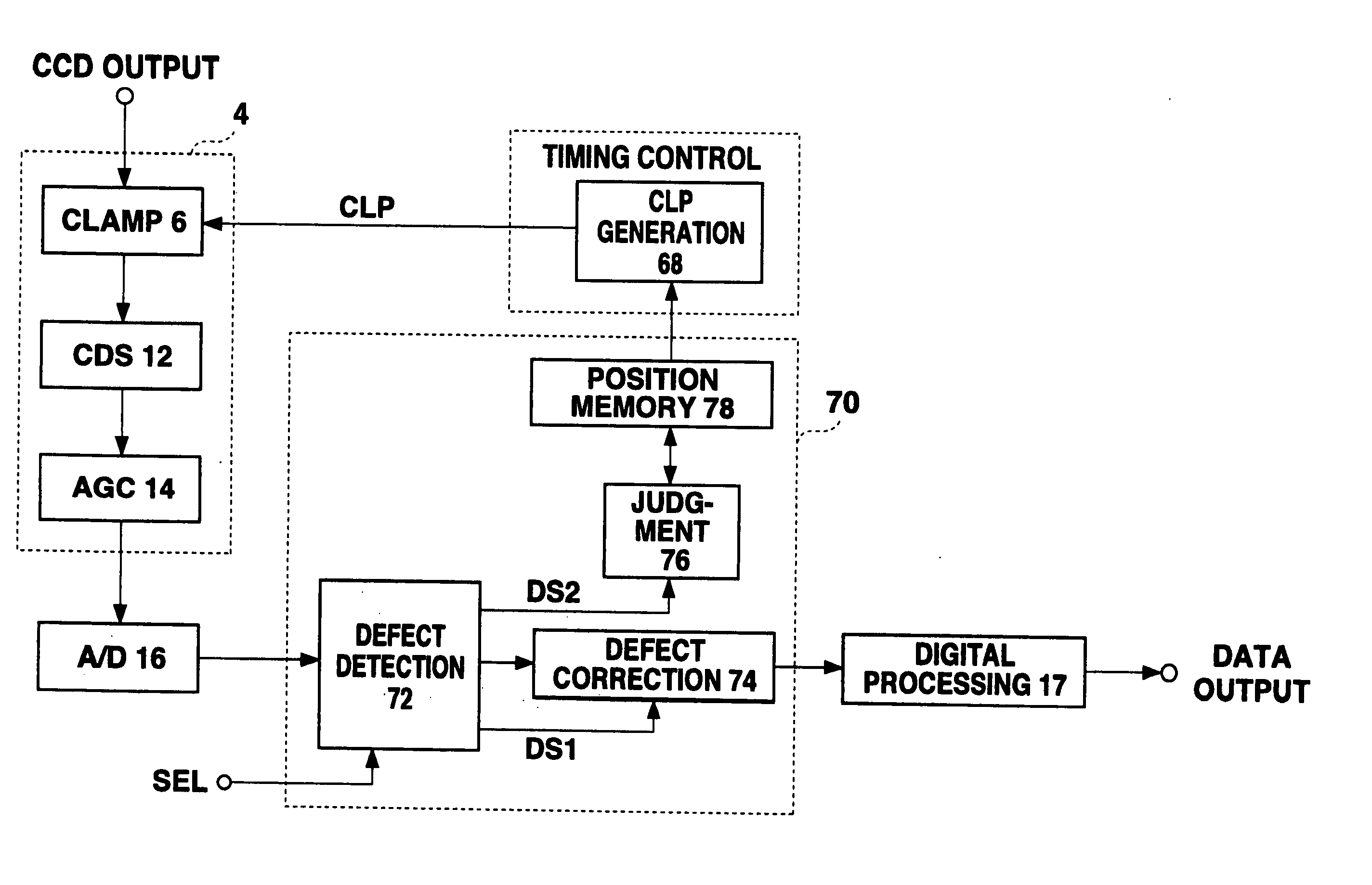
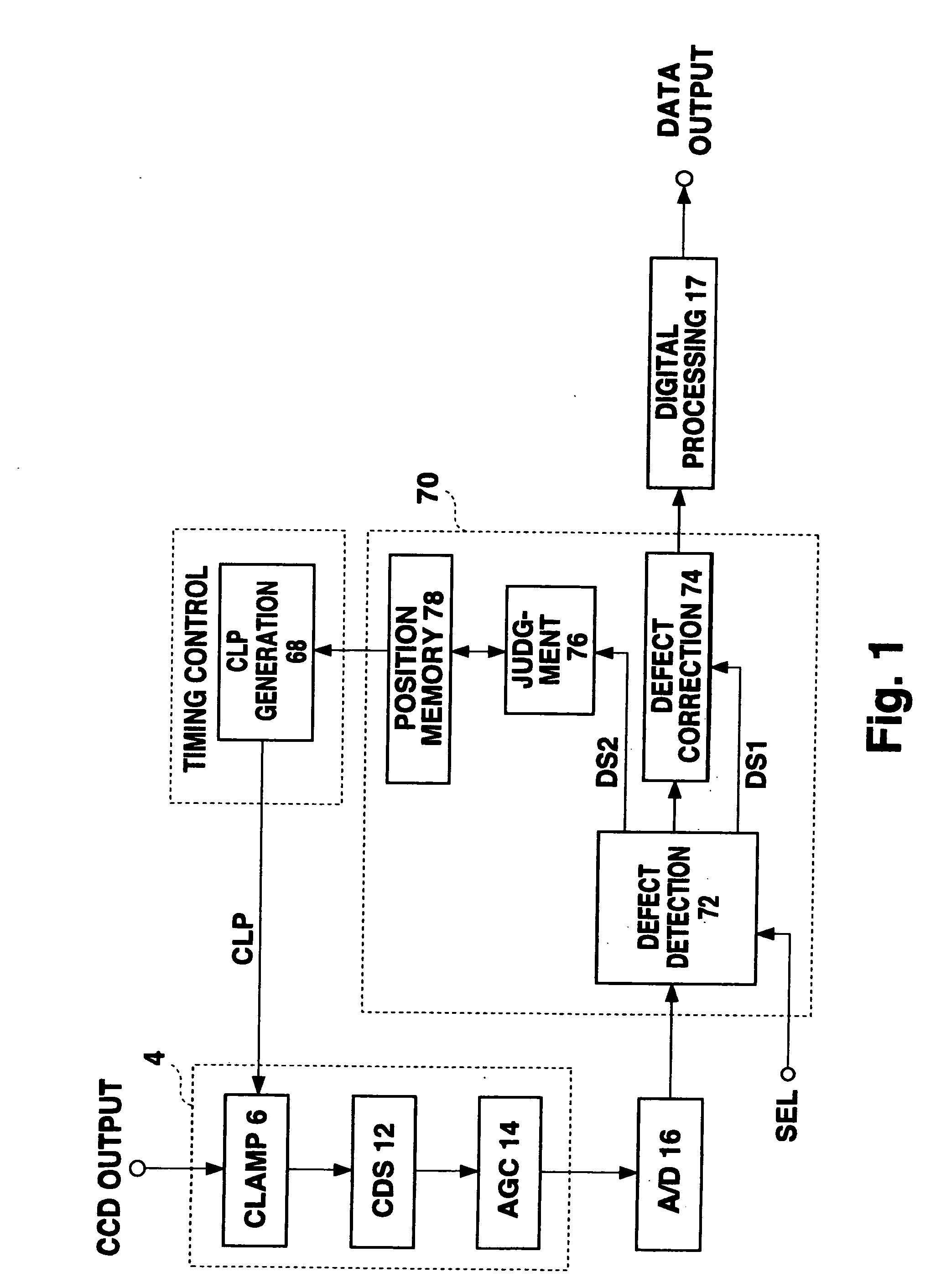
[0026]FIG. 1 is a block diagram showing the configuration of an embodiment of the present invention. In the drawing, the same components as those of the configuration shown in FIG. 8 are denoted by the same reference marks as those of the configuration shown in FIG. 8.

[0027] A signal processing apparatus 1 shown in FIG. 1 includes the analog processing circuit 4, the A / C conversion circuit 16, a defect processing circuit 70, the clamp pulse generation circuit 68 and the digital processing circuit 17. The analog processing circuit 4 is composed of the clamp circuit 6, the CDS circuit 12 and the AGC circuit 14. The analog processing circuit 4 performs the predetermined analog signal processing of the CCD output signal Y(t). The clamp circuit 6 clamps the black reference value B(t) included in the CCD output signal Y(t) in response to the clamp pulse CLP output from the clamp pulse generation circuit 68, and fixes the electric potential of all of the black levels of the CCD output sig...


PUM


Abstract

A signal processing apparatus including a clamp pulse generation circuit for generating a clamp pulse in synchronization with an image signal, a clamp circuit for clamping a signal of a black reference value in response to the clamp pulse, and a defect detection circuit for detecting a defective pixel included in an optical black area, wherein the clamp pulse generation circuit cancels a rise of the clamp pulse when a position of the defective pixel detected by the defect detecting circuit and a position of a rise state of the clamp pulse overlap with each other.

Description

CROSS-REFERENCE TO RELATED APPLICATION [0001] The entire disclosure of Japanese Patent Application No. 2003-331851 including specification, claims, drawings and abstract is incorporated herein by reference in its entirety. BACKGROUND OF THE INVENTION [0002] 1. Field of the Invention [0003] The present invention relates to a signal processing apparatus for detecting a defective pixel included in a light-receiving pixel area and an optical black area of an imaging device to correct the detected defective pixel. [0004] 2. Description of the Related Art [0005]FIG. 8 is a block diagram showing the configuration of a conventional imaging device. The imaging device shown in FIG. 8 includes an analog processing circuit 4, a clamp pulse generation circuit 68, an A / D conversion circuit 16 and a digital processing circuit 17. [0006] As shown in FIG. 9, in a CCD solid-state imaging device, a plurality of light-receiving pixels are arranged in a matrix to form a light-receiving pixel area 2i, in...

Claims


Application Information

Patent Timeline
IPC IPC(8): H01L27/14H01L27/148H01L29/765H04N5/335H04N5/341H04N5/367H04N5/369H04N5/372H04N5/378H04N9/64
CPCH04N5/3675H04N5/361H04N25/683H04N25/63H04N25/60H04N25/68
Inventor MATSUYAMA, HISASHIWATANABE, TOHRU
Owner SEMICON COMPONENTS IND LLC
Why Eureka
Try Eureka