Semiconductor process and yield analysis integrated real-time management method

a technology of real-time management and semiconductor process, applied in the field of management methods, can solve the problems of difficult monitoring of the performance of the semiconductor process b>10/b>, no effective integration methods, and difficult selection of effective data from the large amount of raw data

Active Publication Date: 2006-08-29
POWERCHIP SEMICON MFG CORP
View PDF8 Cites 20 Cited by
  • Summary
  • Abstract
  • Description
  • Claims
  • Application Information

AI Technical Summary

Benefits of technology

[0007]It is an advantage of the claimed invention that the semiconductor process and yield analysis integrated real-time management method can transfer the inspecting results of semiconductor process to all kinds of tables and charts for providing management and analysis. The tables and charts are integrated to present on the web page according to the management classes, which provides real-time interactive monitor and management.

Problems solved by technology

In the prior art, there are no effective ways to integrate these raw data generated in each steps, therefore it is difficult to monitor the performance of the semiconductor process 10.
For different management classes, it is also hard to select the effective data from the large amount of the raw data.

Method used


Image

  • Semiconductor process and yield analysis integrated real-time management method
  • Semiconductor process and yield analysis integrated real-time management method
  • Semiconductor process and yield analysis integrated real-time management method

Examples


Embodiment Construction

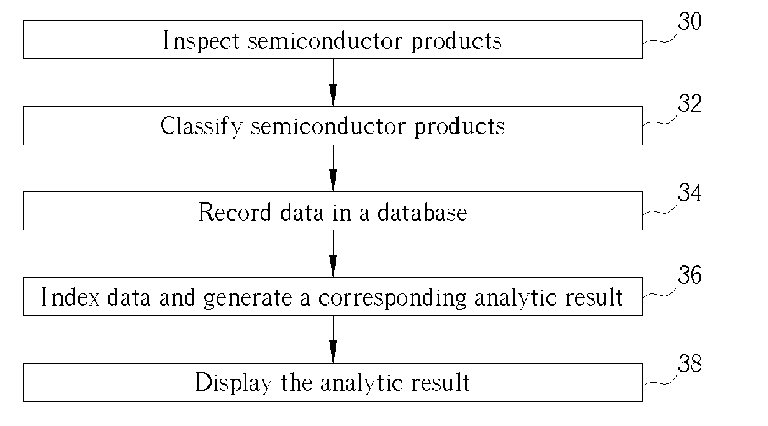
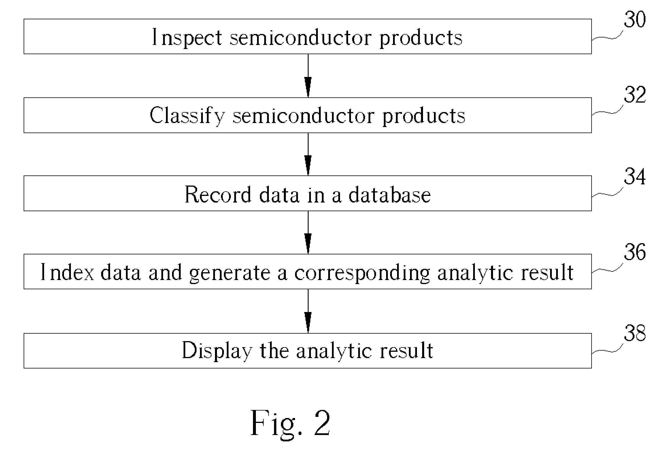
[0019]Please refer to FIG. 2. FIG. 2 is a diagram of semiconductor process and yield analysis management method according to the present invention. The method includes the following steps:

[0020]step 30: inspecting a plurality of semiconductor products with a plurality of items during semiconductor process, and recording a plurality of inspecting results of each semiconductor product;

[0021]step 32: classifying the semiconductor products as a plurality of groups with a default rule, generating raw data according to the inspecting results of each group;

[0022]step 34: recording the raw data and the corresponding groups in a database;

[0023]step 36: indexing a plurality of semiconductor product groups from the database by a default product rule, indexing the corresponding raw data of each semiconductor product group by default parameters, and calculating a corresponding analysis result from the indexed semiconductor product groups and raw data with analysis modules; and

[0024]step 38: disp...


PUM


Abstract

A semiconductor process and yield analysis integrated real-time management method comprises inspecting a plurality of semiconductor products with a plurality of items to generate and record a plurality of inspecting results during semiconductor process, classifying the semiconductor products as a plurality of groups with a default rule to generate and record an initial data in a database, indexing a plurality of semiconductor product groups and the corresponding initial data from the database by a default product rule and parameter to calculate a corresponding analysis result, and displaying the analysis result according to the indexed semiconductor product groups and the initial data.

Description

BACKGROUND OF INVENTION[0001]1. Field of the Invention[0002]The present invention relates to a management method, and more particularly, to an integrated real-time management method which provides semiconductor process and yield analysis for a plurality of management classes.[0003]2. Description of the Prior Art[0004]A lot of data are used in the semiconductor process to monitor, control and improve all kinds of manufacturing processes. Please refer to FIG. 1; FIG. 1 is a block diagram of a semiconductor process 10 according to the prior art. The semiconductor process 10 processes a plurality of wafers 12 through seven steps, including a step of thin film 14, a step of diffusion 16, a step of photo 18, a step of etch 20, a sample test 22, a wafer test 24, and a final test 26. A plurality of inspecting results are generated in each step to control and improve the semiconductor process 10. However, the inspecting results are merely raw data. In the prior art, there are no effective wa...

Claims


Application Information

Patent Timeline
Patent Type & Authority Patents(United States)
IPC IPC(8): G06F19/00G05B19/418G05B23/02H01L21/02
CPCH01L22/20G05B2219/32191Y02P90/02
Inventor TAI, HUNG-ENCHEN, CHIEN-CHUNGWANG, SHENG-JEN
Owner POWERCHIP SEMICON MFG CORP
Why Eureka
Try Eureka