High speed connector assembly with laterally displaceable head portion

a connector and assembly technology, applied in the direction of connection contact member material, two-part coupling device, connection device connection, etc., can solve the problems of significant mismatch between connectors of each connector assembly, misalignment giving rise to mechanical stress between the connectors and printed circuit boards, and increase the difficulty of noise-free communication of electrical signals, so as to reduce the damage of surface mount connector-to-printed circuit board connections, prevent the transfer of stress, and reduce the effect of stress

Inactive Publication Date: 2006-10-17
CNPLUS
View PDF40 Cites 17 Cited by
  • Summary
  • Abstract
  • Description
  • Claims
  • Application Information

AI Technical Summary

Benefits of technology

[0025]By allowing the head portion of the second connector to be laterally displaceable with respect to the body portion of the second connector, the connector assembly can prevent stress from being transferred to the surface-mount connections between the first connector and the first printed circuit board and between the second connector and the second printed circuit board. By preventing or reducing this stress, damage to the surface mount connector-to-printed circuit board connections is reduced or avoided. Relatively fragile solder surface mount techniques and structures can therefore be employed to couple the connectors to their respective printed circuit boards without unacceptable high failure rates of the surface mount joints.
[0026]The contact beam and conductor structure of the mating PC portions in the connector assembly is fashioned to shield signal conductors and signal contact beams with ground conductors. By having a PC portion signal conduction path in one connector and a PC portion signal conduction path in the second connector, the same PC materials and conductor dimensions and ground planes are provided in both connectors. Changes in the characteristic impedance of the signal path as the signal path extends from one connector to the other connector is reduced, thereby reducing unwanted reflections. By using surface-mount structures (for example, solder balls or metal surface mount contacts) to surface-mount the first edges of the PC portions to their respective printed circuit boards, unwanted extending plated through holes need not be used in the printed circuit board. The extending conductors of contact tails of press-fit pins are also avoided. The associated cross-talk and electromagnetic radiation and reception due to extending plated through holes and contact tails are therefore eliminated due to the use of surface-mount connections to the printed circuit boards.

Problems solved by technology

As operating speeds of the electronics of such electronic equipment and devices have increased, the communication of the electrical signals in a noise-free fashion has become more important and more difficult to achieve.
These reflections are undesirable and may obscure the desired signal that was to be conducted down the conductor.
Again, the induced signal is undesirable and may obscure a desired signal that was to be conducted down the other conductor.
This is undesirable as well.
Although this type of connector assembly works well in many environments, there exist problems in certain applications due to mismatches between connectors when motherboard and daughterboard connectors are brought together when printed circuit boards of electronic equipment are to be connected to one another. FIG. 9 (Prior Art) illustrates one such problem.
When daughterboard 3 and motherboard 2 are brought together, there can be a significant mismatch between connectors of each connector assembly.
When the connectors are mated, the misalignment gives rise to mechanical stress between the connectors and the printed circuit boards to which they are attached.
As signal frequencies increase, however, the length of such a contact tail and the associated plated through hole and the irregular shape and discontinuous electrical characteristics of the contact tail and plated through hole cause electrical reflections, cross-talk and / or electromagnetic radiation.
Although strong and reliable, the structure of FIG. 10 is undesirable due to its electrical characteristics.
It is therefore difficult or impossible to employ the surface mount techniques in high speed connector assemblies involving many signal pairs where there may be multiple connectors on each printed circuit board.

Method used


Image

  • High speed connector assembly with laterally displaceable head portion
  • High speed connector assembly with laterally displaceable head portion
  • High speed connector assembly with laterally displaceable head portion

Examples


Embodiment Construction

[0069]Reference will now be made in detail to some embodiments of the invention, examples of which are illustrated in the accompanying drawings.

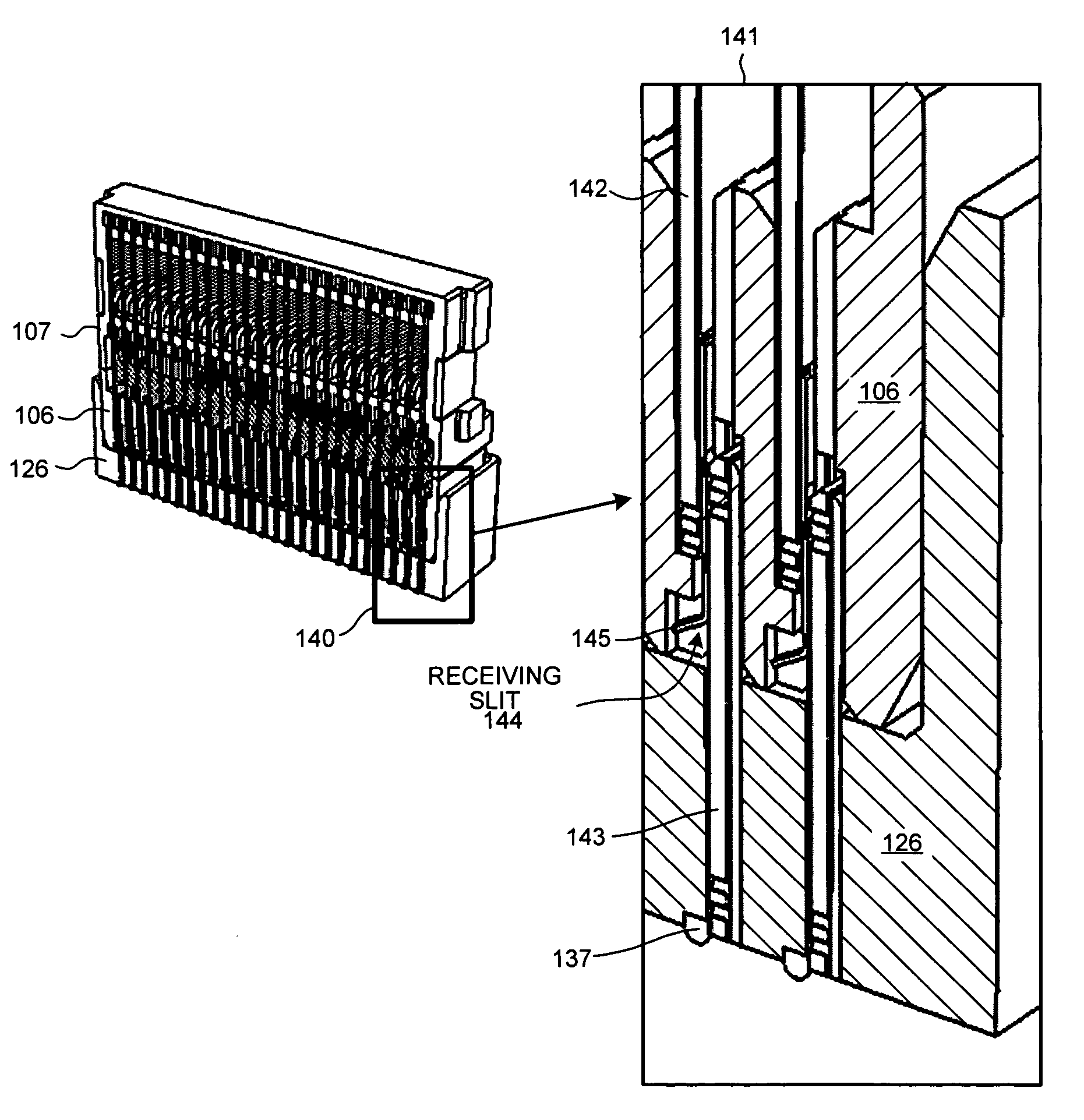
[0070]FIG. 14 is a perspective view of a right angle connector assembly 100 in accordance with one novel embodiment. Connector assembly 100 includes a first connector 101 and a second connector 102. First connector 101 may, for example, be attached to a motherboard printed circuit board whereas second connector 102 may be attached to a daughterboard printed circuit board. First connector 101 is therefore hereinafter referred to as a motherboard connector and second connector 102 is hereinafter referred to as a daughterboard connector. To couple the two connectors 101 and 102 together, the second connector 102 may be moved in the direction of arrow 103 with respect to connector 101.

[0071]FIG. 15 is a perspective view of daughterboard connector 102. Ribs 104 of connector 102 slidingly engage corresponding guide groves 105 in connector 101 when...


PUM


Abstract

A high speed connector assembly includes a first surface-mount connector (SMC) and a second SMC. The first SMC includes a first flexible printed circuit (FPC) that has conductors that extend from a first FPC edge to a second FPC edge. The first edge includes surface-mount contact structures for surface mounting to a first printed circuit board. The second SMC includes a second FPC that has conductors that extend from a first FPC edge to a second FPC edge. The first edge includes surface-mount contact structures for surface mounting to a second printed circuit board. A set of contact beams is disposed along the second FPC edge. The first and second SMCs are mateable such that the contact beams make electrical contact between conductors in the first FPC and conductors in the second FPC. The FPC of the second SMC flexes to adjust for misalignments between the first and second SMCs.

Description

CROSS REFERENCE TO RELATED APPLICATION[0001]This application is a continuation in part of, and claims priority under 35 U.S.C. §120 from, nonprovisional U.S. patent application Ser. No. 11 / 128,149 entitled “High Speed Connector Assembly With Laterally Displaceable Head Portion,” filed on May 11, 2005 now U.S. Pat. No. 6,986,682, the subject matter of which is incorporated herein by reference.TECHNICAL FIELD[0002]The present invention relates generally to high speed connectors.BACKGROUND INFORMATION[0003]Electrical connectors are used in electronic equipment and devices to communicate electrical signals from one printed circuit board to another. As operating speeds of the electronics of such electronic equipment and devices have increased, the communication of the electrical signals in a noise-free fashion has become more important and more difficult to achieve. If, for example, an electrical signal is transmitted down a conductor and if there are discontinuities in the characteristi...

Claims


Application Information

Patent Timeline
Patent Type & Authority Patents(United States)
IPC IPC(8): H01R13/648
CPCH01R23/6873H01R12/592H01R12/79H01R12/721H01R13/658
Inventor JEON, MYOUNGSOO
Owner CNPLUS
Why Eureka
Try Eureka