

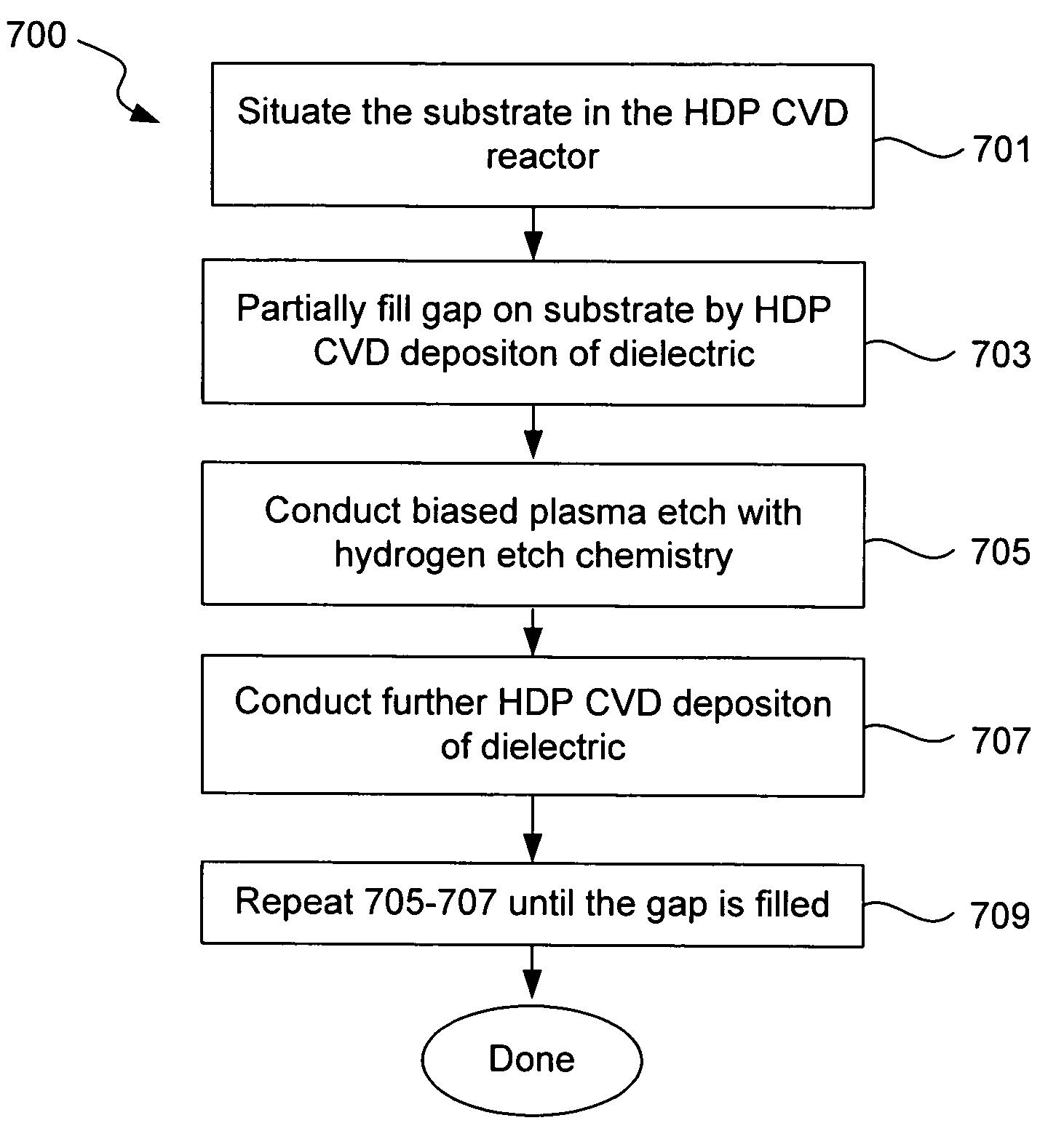
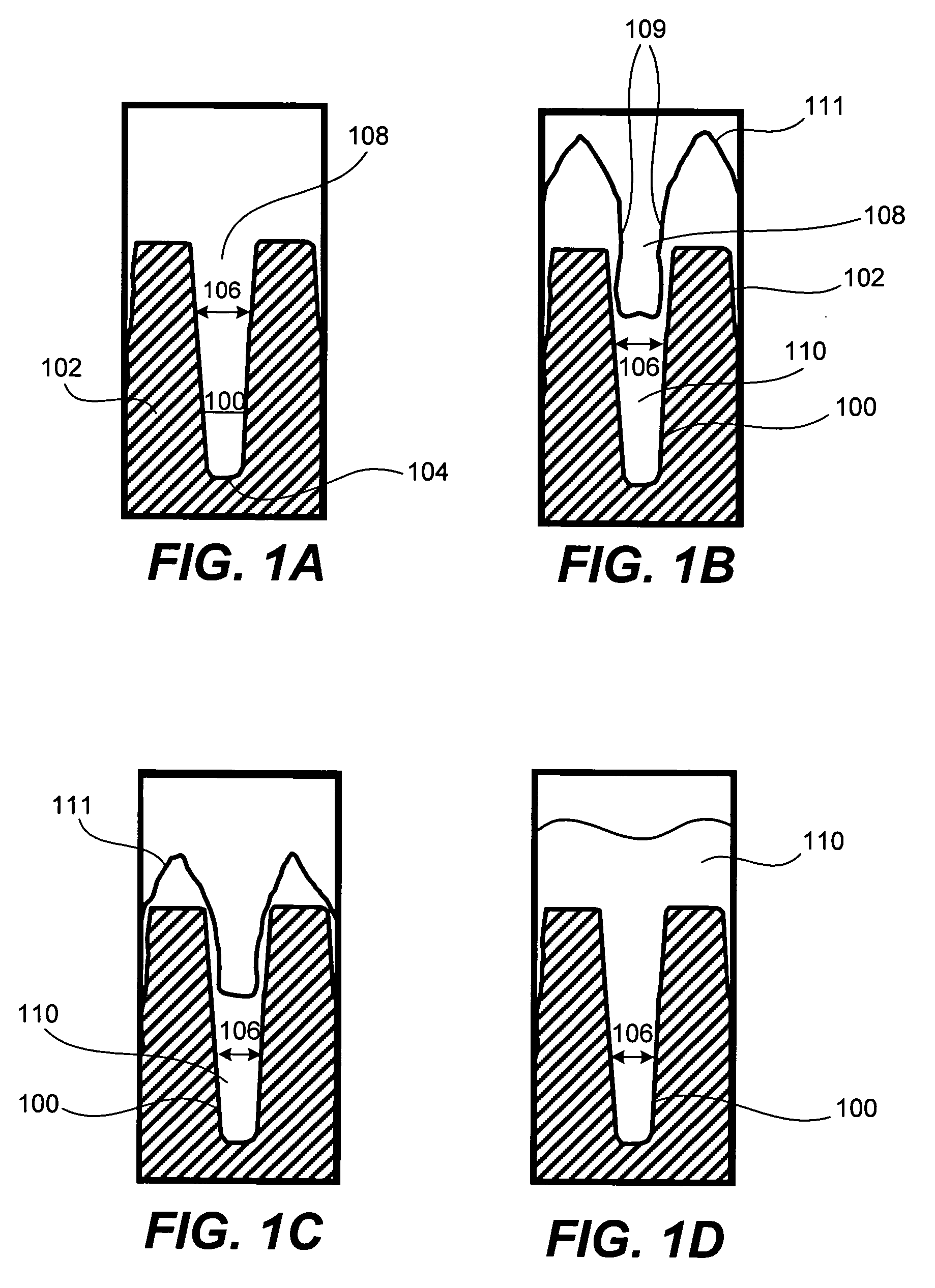
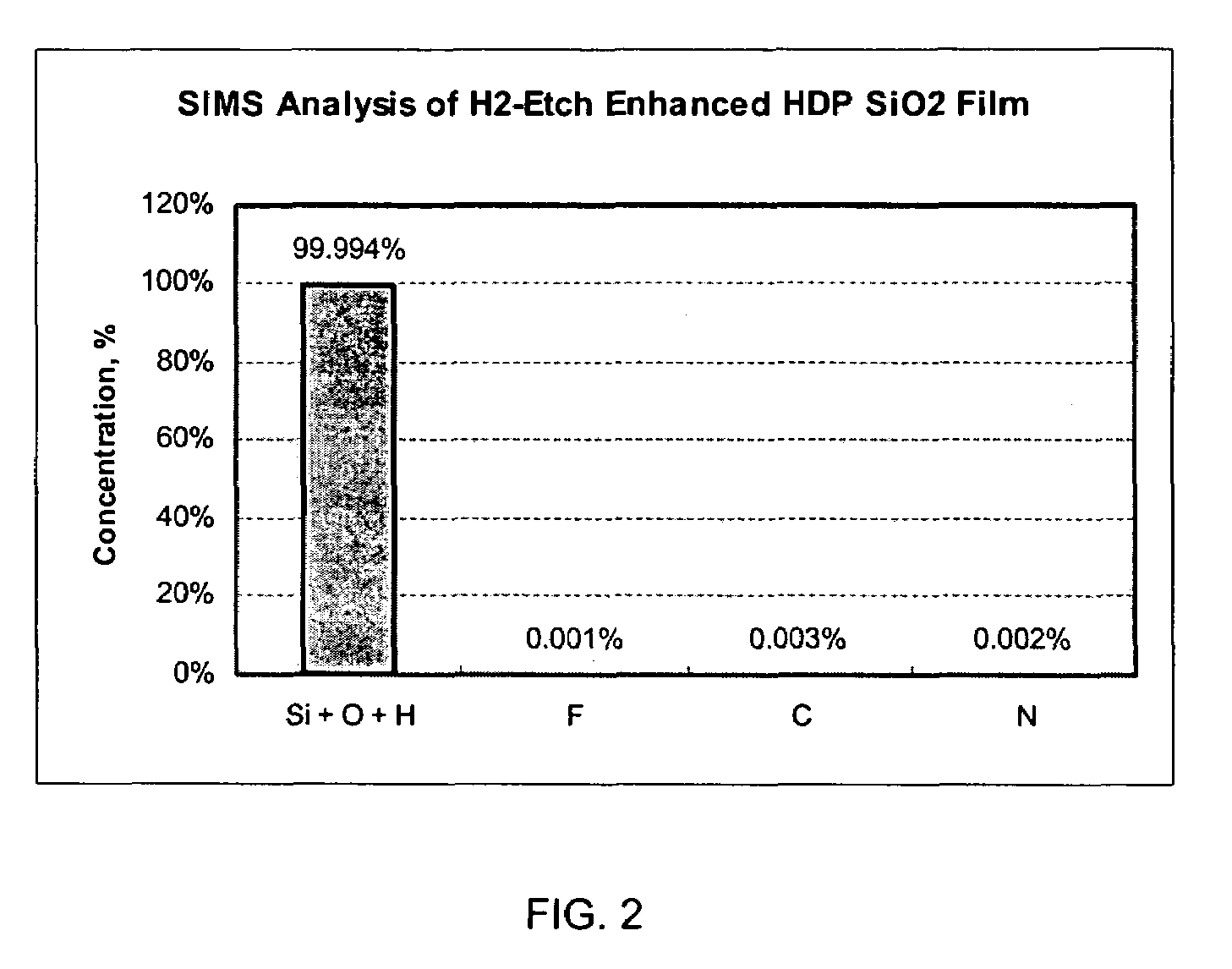
Biased H2 etch process in deposition-etch-deposition gap fill
a technology of etching and h2 etching, which is applied in the direction of semiconductor/solid-state device manufacturing, basic electric elements, electric apparatus, etc., can solve the problems of increasing difficulty in cvd diffusion, and increasing difficulty in void-free filling of narrow width, etc., to reduce or eliminate the effect of dielectric contamination
- Summary
- Abstract
- Description
- Claims
- Application Information
AI Technical Summary
Benefits of technology
Problems solved by technology
Method used
Image

Examples
Embodiment Construction
[0020]Reference will now be made in detail to specific embodiments of the invention. Examples of the specific embodiments are illustrated in the accompanying drawings. While the invention will be described in conjunction with these specific embodiments, it will be understood that it is not intended to limit the invention to such specific embodiments. On the contrary, it is intended to cover alternatives, modifications, and equivalents as may be included within the spirit and scope of the invention as defined by the appended claims. In the following description, numerous specific details are set forth in order to provide a thorough understanding of the present invention. The present invention may be practiced without some or all of these specific details. In other instances, well known process operations have not been described in detail in order not to unnecessarily obscure the present invention.
[0021]Introduction
[0022]The present invention relates to chemical vapor deposition and b...
PUM
 Abstract
Description
Claims
Application Information