
STM mapping circuit and method

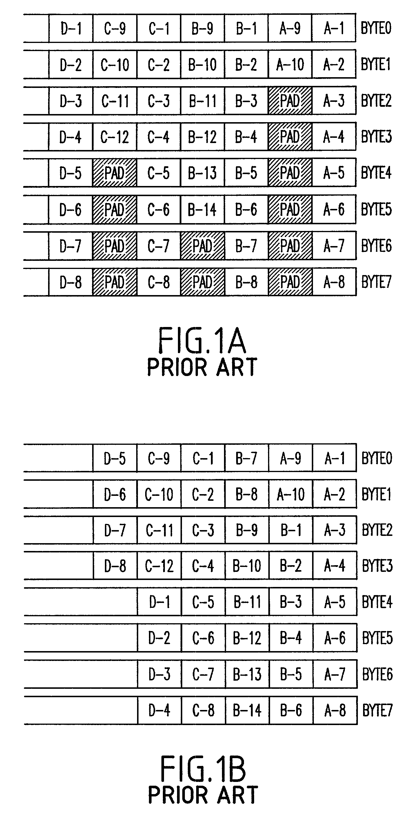
a mapping circuit and circuit technology, applied in the field of stm mapping circuits, can solve the problems of limited transmission bit rate, signal processing speed of transmission devices, and no proposal has been made regarding a specific method of eliminating pad bytes

Inactive Publication Date: 2007-02-06
NEC CORP
View PDF5 Cites 2 Cited by
  • Summary
  • Abstract
  • Description
  • Claims
  • Application Information

AI Technical Summary

Benefits of technology

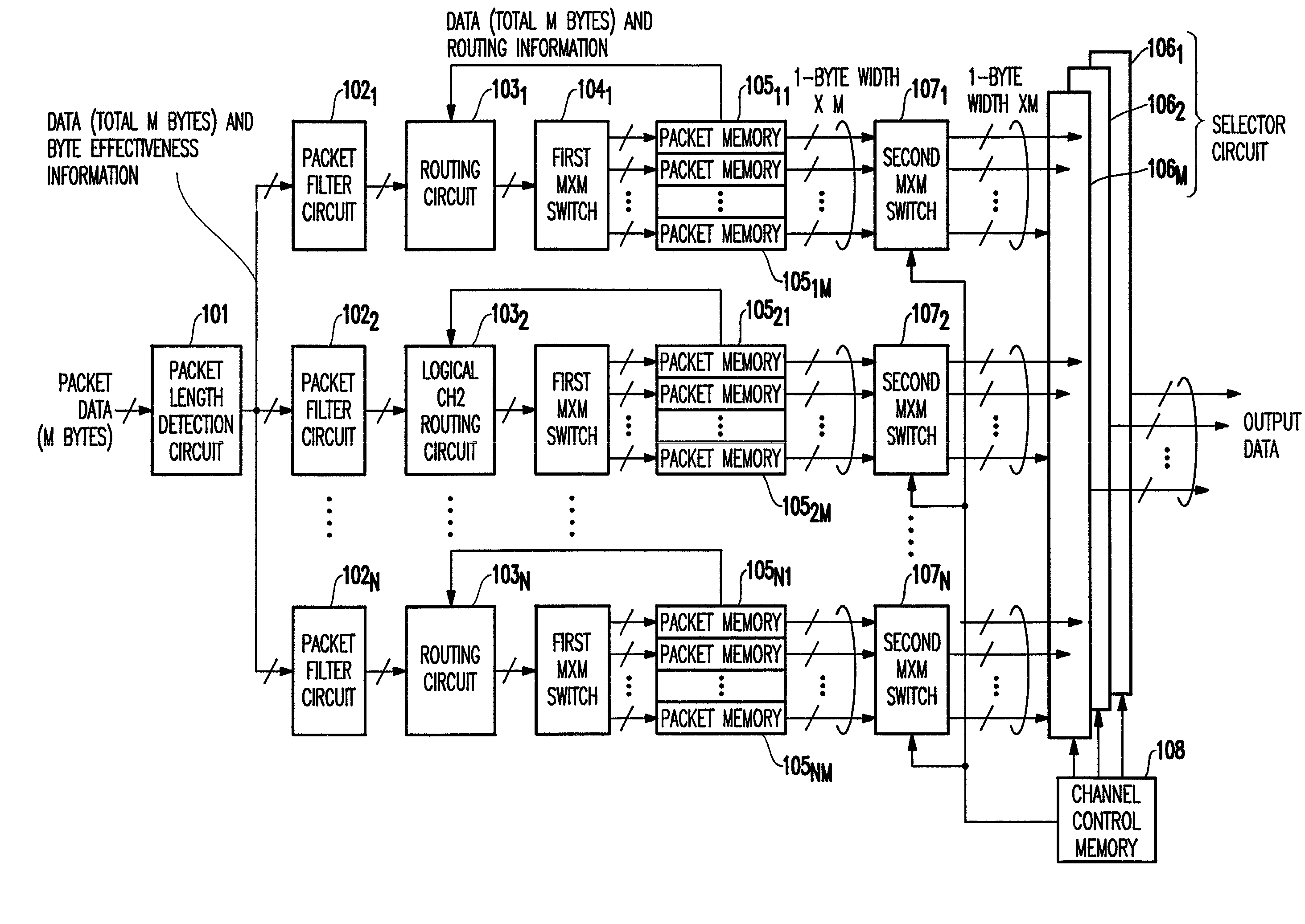
The present invention aims to solve the problem of prior art by providing an STM mapping circuit that can map packet data without eliminating pad bytes. This results in more efficient data processing.

Problems solved by technology

The patent text discusses the problem of unnecessary data, such as pad bytes, that take up bandwidth in communication lines. The text proposes a method for eliminating these unnecessary data, but there is no specific proposal for this purpose. The text also mentions the use of STM mapping circuits that can eliminate pad bytes, but these circuits are not widely used in practical applications. The technical problem is to provide a more efficient and effective method for eliminating unnecessary data, such as pad bytes, in communication lines.

Method used


Image

  • STM mapping circuit and method
  • STM mapping circuit and method
  • STM mapping circuit and method

Examples


first embodiment

[0067]The first embodiment of the STM mapping circuit of the present invention is next described with reference to the accompanying figures.

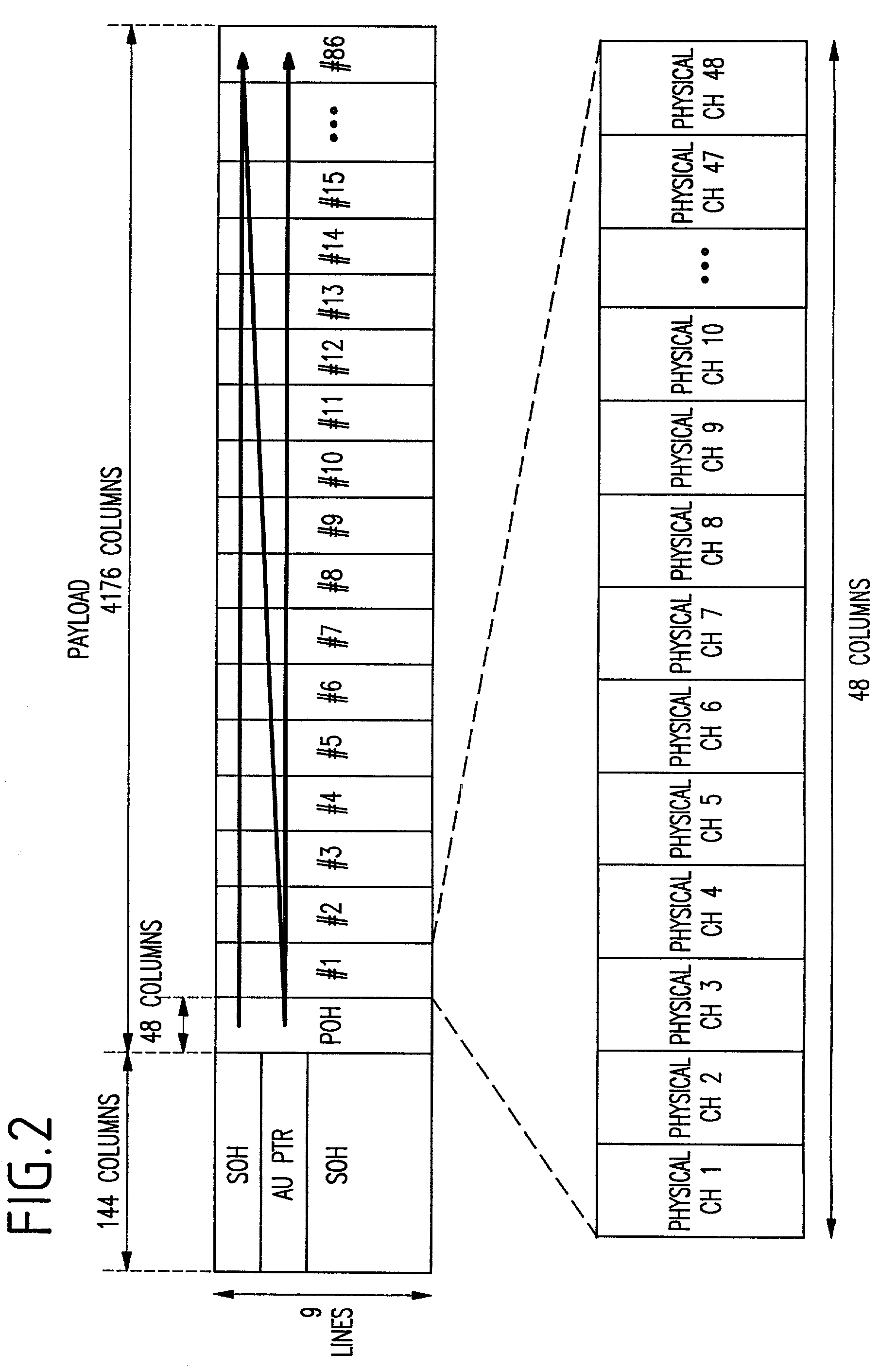
[0068]We refer now to FIG. 2, which is a schematic diagram showing an example of the constitution of a transmission frame. STS-n is a multiplexing format that is prescribed for a SONET (Synchronous Optical Network), and STM-n is a multiplexing format that is prescribed for SDH (Synchronous Digital Hierarchy).

[0069]As shown in FIG. 2, an STS or STM transmission frame is constituted such that SOH (Section Over Head) areas and an AU PTR (Administrative Unit Pointer) area are provided at the head, and payload areas (including POH (Path Over Head) areas) are provided following this head.

[0070]In the case of STM-16, for example, the payload area is made up by 48 AU-3 (51.84 Mbps), and if one physical channel is assigned to AU-3 , a maximum of 48 physical channel byte data are stored in the payload area. The byte data of each physical channel are store...

second embodiment

[0121]Explanation is next presented regarding the second embodiment of the STM mapping circuit of the present invention with reference to the accompanying figures.

[0122]In the STM mapping circuit shown in the first embodiment, first M×M switches 1041–104N are constituted by a number M of M→1 selector circuits, and the M→1 selector circuits are in turn constituted by (M−1) 2→1 selector circuits.

[0123]Accordingly, a number M ((M−1) of 2→1 selector circuits are required to constitute first M×M switches 1041–104N, the number of 2→1 selector circuits required to constitute the first M×M switches increasing as M increases. In the present embodiment, an STM mapping circuit is proposed that enables a reduction in the circuit scale.

[0124]We now refer to FIG. 8, which is a block diagram showing the configuration of the second embodiment of the STM mapping circuit of the present invention.

[0125]As shown in FIG. 8, the STM mapping circuit of this embodiment is a configuration that includes:

[012...


PUM


Abstract

An STM mapping circuit is disclosed having a configuration that includes: a packet length detection circuit for generating byte effectiveness information that indicates whether byte data are effective data or not; routing circuits for generating routing information for rearranging byte data in a prescribed order while using byte effectiveness information to eliminate pad bytes; packet filter circuits for taking in packet data for each logical channel in accordance with channel number signals that indicate which logical channel the packet data belong to; M×M switches for sorting packet data for logical channel in a prescribed order while removing pad bytes in accordance with routing information; and packet memories that hold, for each logical channel, packet data that have been sorted by the M×M switches.

Description


Claims


Application Information

Patent Timeline
Owner NEC CORP
Learn More