Step-over lithography to produce parabolic photoresist profiles for microlens formation

a technology of parabolic photoresist and microlens, applied in the field of image sensing devices, can solve the problems of repeatability and aberration of lens shapes, and the optimum design of one color may not be quite right for another color, so as to improve reproducibility and accuracy, the effect of improving the shap

Inactive Publication Date: 2007-03-13
SHARP KK
View PDF6 Cites 1 Cited by
  • Summary
  • Abstract
  • Description
  • Claims
  • Application Information

AI Technical Summary

Benefits of technology

[0011]It is an object of the invention to provide a method to generate improved shapes in photoresist having better reproducibility and accuracy using photolithographic techniques.
[0012]Another object of the invention is to provide a technique which allows customized shapes for the lens for each color.

Problems solved by technology

Lens shape repeatability and aberrations caused by distortions are common problems using such techniques.
Another problem with lens stack design is that an optimum design for one color may not be quite right for another color.

Method used


Image

  • Step-over lithography to produce parabolic photoresist profiles for microlens formation
  • Step-over lithography to produce parabolic photoresist profiles for microlens formation
  • Step-over lithography to produce parabolic photoresist profiles for microlens formation

Examples


Embodiment Construction

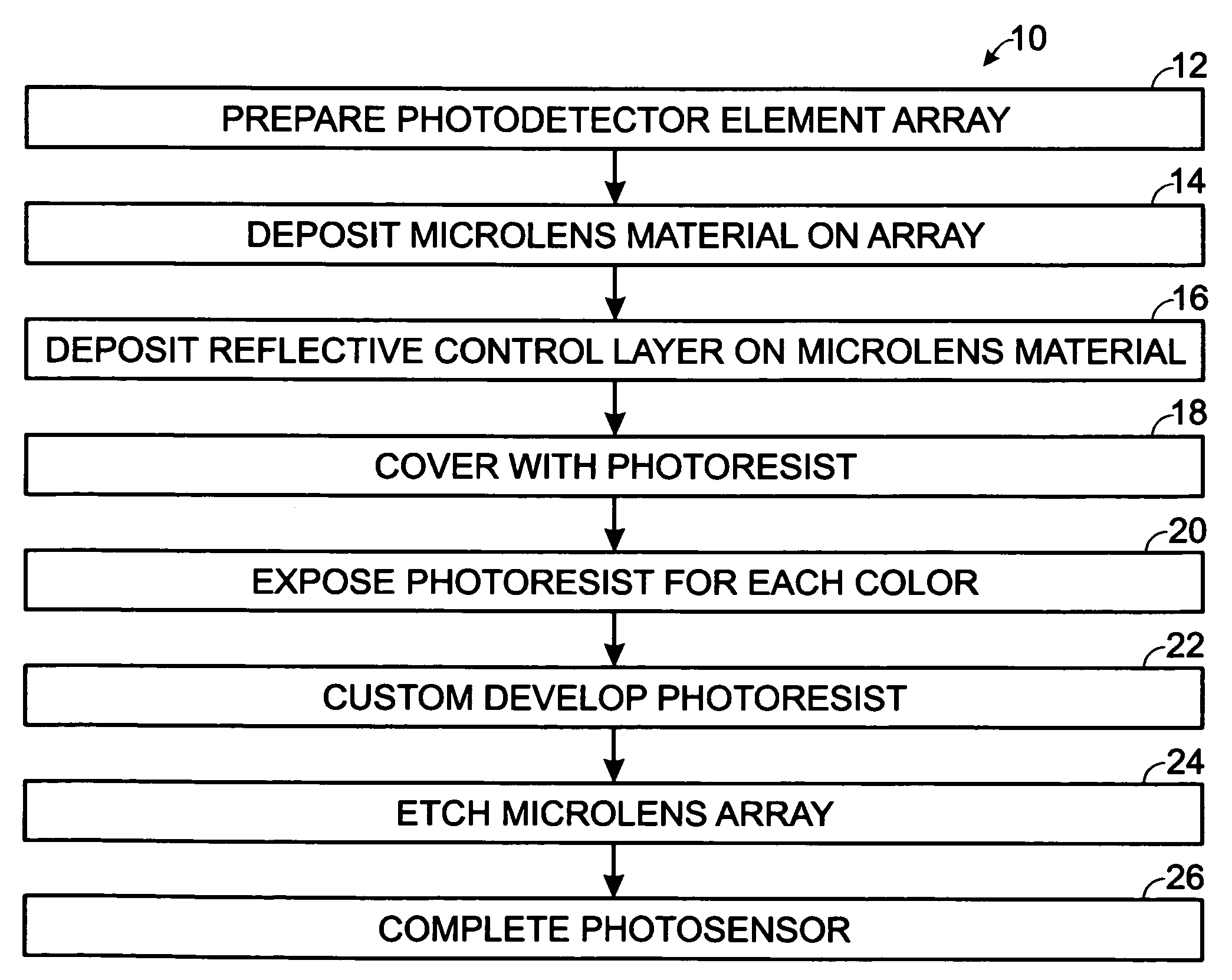
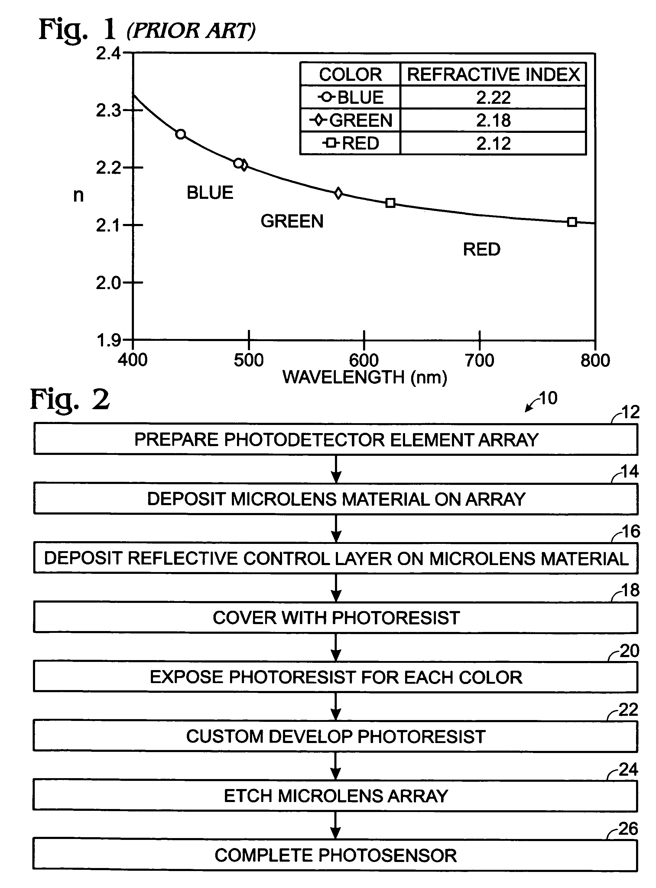
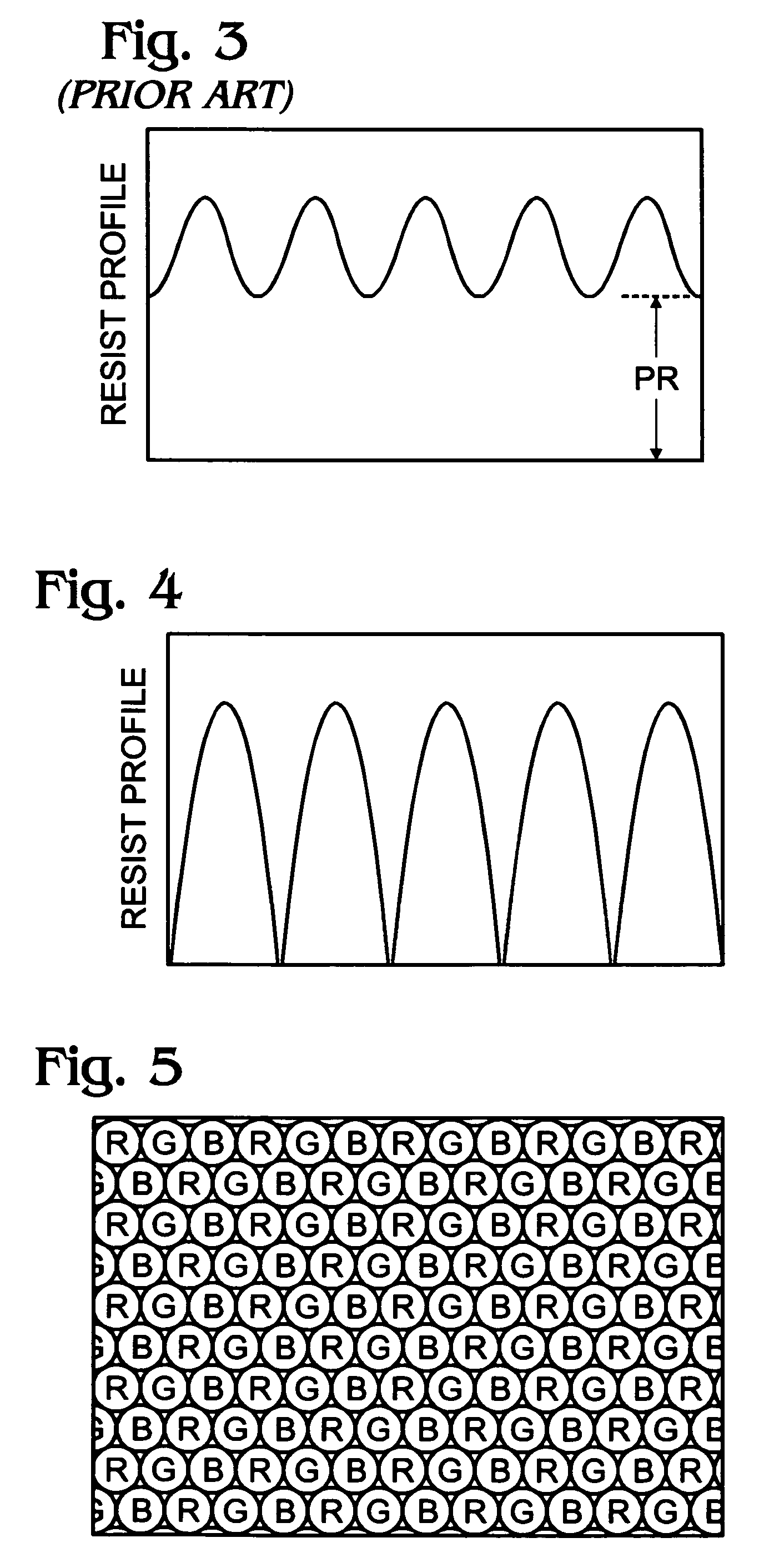
[0023]A method is disclosed to generate improved shapes in photoresist having better reproducibility and accuracy using photolithographic techniques with parameters that can be programmed into a stepper. This also allows customized shapes for the lens for each color of a color domain, thereby optimizing the focal point for, e.g., blue, green, and red photons, independent of each other.

[0024]The objective of the invention is to produce convex lens shapes in a high refractive index material for the purpose of concentrating photons impinging on the surface of a film onto the active photodectector element. This method offers the advantage of better reproducibility and possibly simpler processing sequences. The dimensions of the lens can be made extremely small, offering scalability to approximately a one-micron diameter. Both convex and concave shapes can be generated in the photoresist, which is then transferred to underlying material through appropriately developed dry etch processes....


PUM

PropertyMeasurementUnit
refractive indexaaaaaaaaaa

Abstract

A method of microlens fabrication for use in a photosensor includes preparing a photodetector element array which is sensitive to light in a specific color domain and depositing microlens material on the photodetector element array. The structure is coated with photoresist, and the photoresist is masked and exposed in a separate exposure for each color in the color domain. The photoresist is developed and the microlens material etched to form a microlens array.

Description

FIELD OF THE INVENTION[0001]This invention relates to image sensing devices, and specifically to improvements in the light collecting efficiency for image sensing in CCD and CMOS imagers.BACKGROUND OF THE INVENTION[0002]The light forming the image that is focused onto an imaging device has an inherent efficiency for detection. The photon flux through an aperture falls onto a sensor surface and is converted into an electrical signal that is stored as one component of a pixel of a digital image. Each pixel of the image is typically composed of either of three individual photodetectors corresponding to a color domain, having three of the fundamental colors, e.g., red, green, blue (RGB) or the complimentary color domain having cyan, magenta, yellow (CMY). The intensity of the electrical signal is roughly proportional to the quantity of photons sensed at each photodetector. A lens, or microlens, is typically used to focus the incoming light into the active area of each photodetector. Lar...

Claims


Application Information

Patent Timeline
Patent Type & Authority Patents(United States)
IPC IPC(8): G02B27/10B29D11/00G03C5/00
CPCB29D11/00365G03F7/0007G02B3/0012
Inventor ULRICH, BRUCE D.ONO, YOSHI
Owner SHARP KK
Why Eureka
Try Eureka