Semiconductor manufacturing system and wafer holder for semiconductor manufacturing system

a semiconductor manufacturing system and semiconductor technology, applied in the field of semiconductor manufacturing system and semiconductor wafer holder, can solve the problems of reducing the uniformity of the backside of the semiconductor wafer, affecting and repeatedly applying mechanical stress to the semiconductor wafer and the slot, so as to improve the yield and productivity of semiconductors

Inactive Publication Date: 2007-04-24
TERASEMICON CO LTD
View PDF23 Cites 390 Cited by
  • Summary
  • Abstract
  • Description
  • Claims
  • Application Information

AI Technical Summary

Benefits of technology

[0011]An object of the present invention is to provide a semiconductor manufacturing system and wafer holder for a semiconductor manufacturing system which improves yield and productivity of semiconductor by fundamentally preventing a semiconductor wafer from being exposed to a process reaction in the semiconductor manufacturing system that uses a dual boat and prevents a film from being deposited on the backside of the wafer by using the wafer holder.

Problems solved by technology

Accordingly, when the wafer is unloaded after a film formation process for manufacturing semiconductor has been completed, a film integrated with a wafer and a slot is destroyed.
In addition, since various films are laminated on the backside, mechanical stress is repeatedly applied to the semiconductor wafer and the semiconductor wafer gets bent.
Since the film uniformity of the backside of the semiconductor wafer is greatly reduced in comparison with the film uniformity of the upper surface of the semiconductor wafer, many processing problems are caused in the proceeding processes, especially photolithography.

Method used


Image

  • Semiconductor manufacturing system and wafer holder for semiconductor manufacturing system
  • Semiconductor manufacturing system and wafer holder for semiconductor manufacturing system
  • Semiconductor manufacturing system and wafer holder for semiconductor manufacturing system

Examples


first embodiment

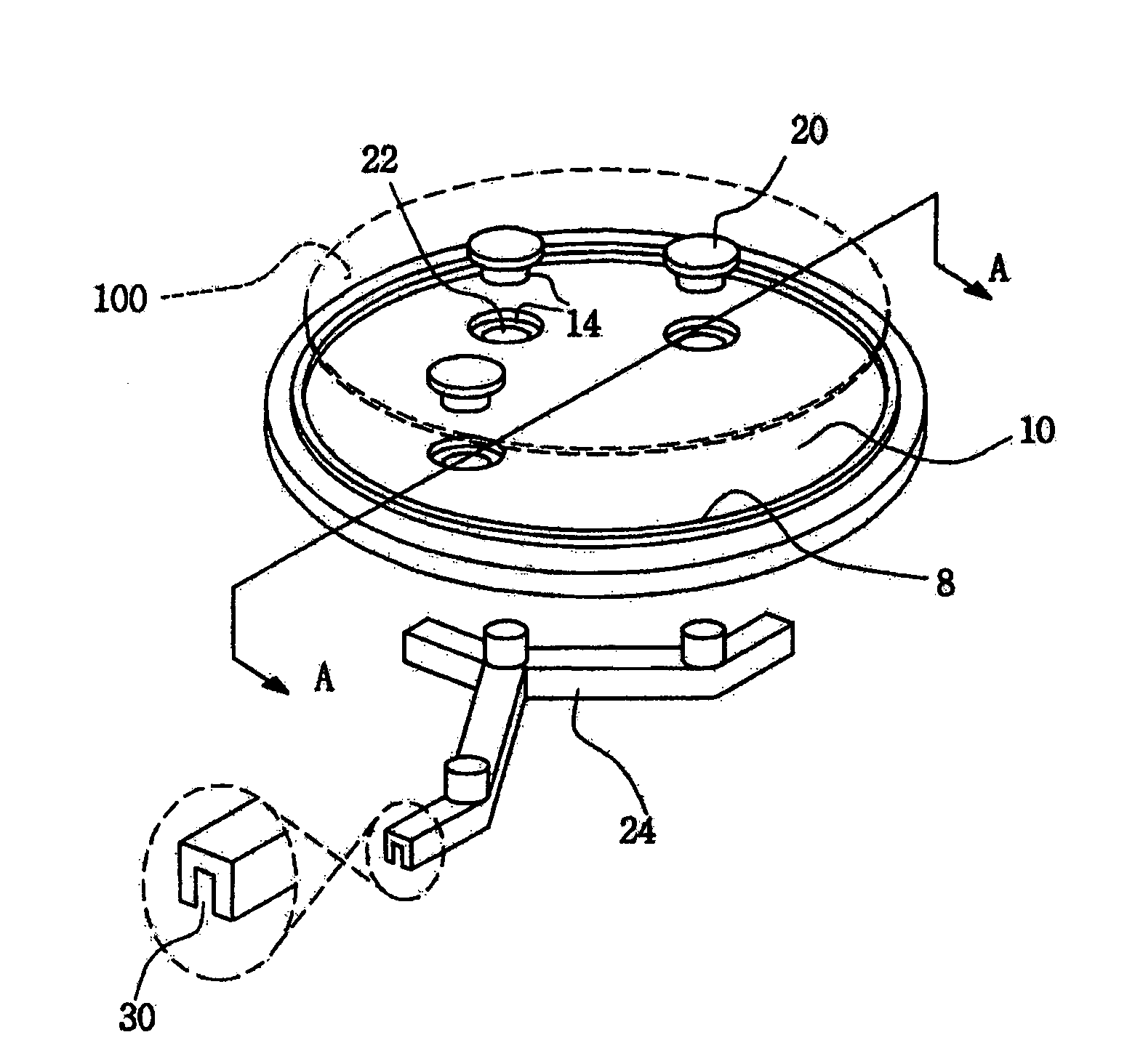
[0047]The present invention is classified into several embodiments according to the wafer lifer 12. FIG. 2A is a perspective view of a wafer holder of the semiconductor manufacturing system according to the present invention. FIGS. 2B1 and 2B2 are cross-sectional views taken along a line A—A in FIG. 2A.

[0048]In the first embodiment, the wafer lifer 12 of the wafer holder includes support poles 20 for supporting at least three points of the semiconductor wafer 100 in a side guard 8 of the holder body 10. The holder body 10 is provided with through holes 22 which the support poles 20 can be inserted into and removed from. The support pole 20 has a lower portion at which a lifting rod 24 operated by a second wafer loading boat 4 is arranged.

[0049]The wafer lifter is a cap type wafer lifter. The support pole 20 that is disengaged has a cap that is lifted from the wafer holder body 10 to support the semiconductor wafer.

[0050]Here, in the cap type case, a tapered surface or a bent and ste...

second embodiment

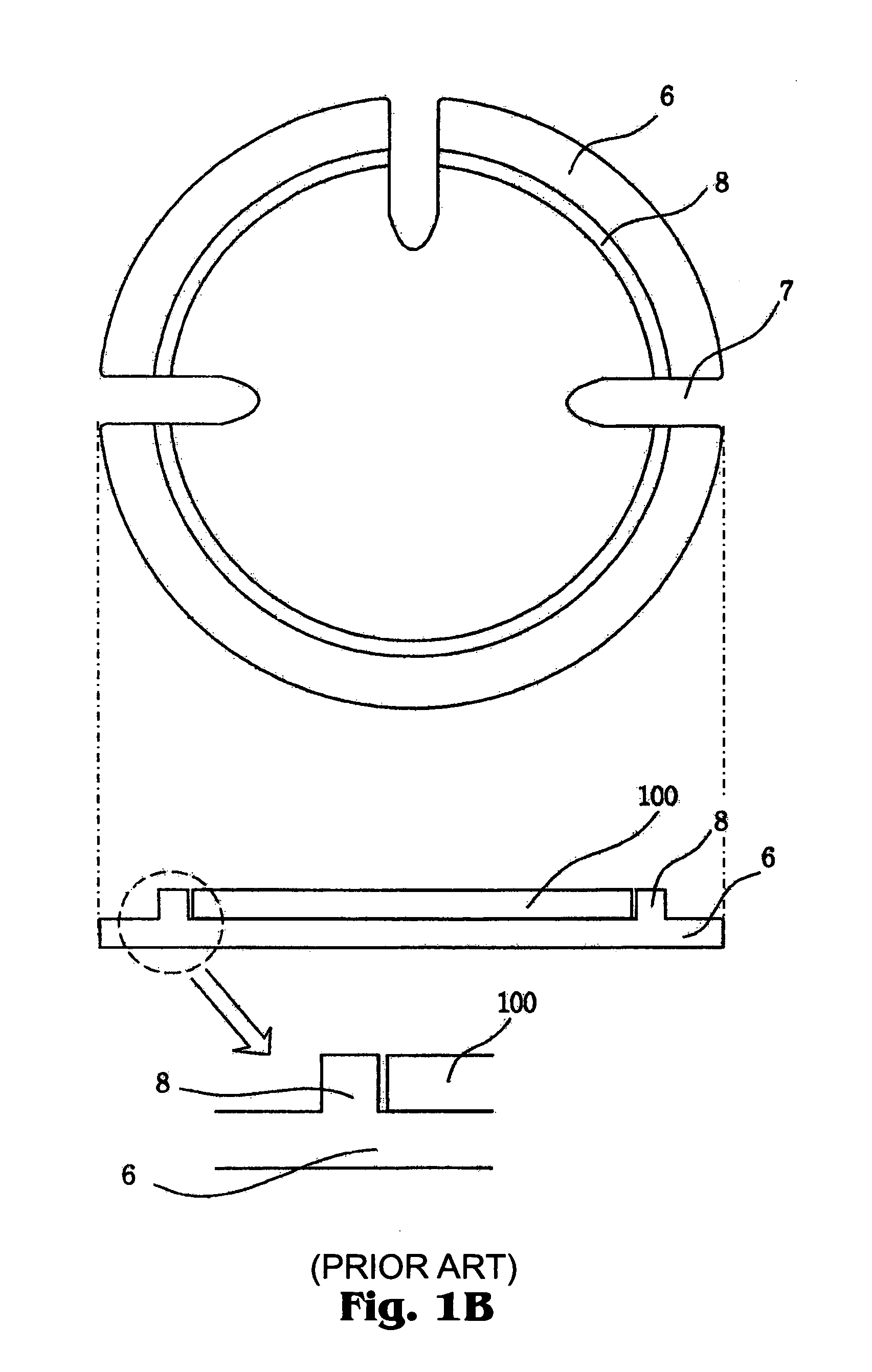
[0070]FIG. 3C is a cross-sectional view of another example of a gas inflow interception surface of the As described above, the gas inflow interception surface 14 is formed to prevent the reaction gas from flowing in through the boundary gap between two separated members. The gas inflow interception surface 14 can be formed as a tapered surface 16 or as a bent and stepped surface 18 as shown in FIG. 3B. The gas inflow interception surface 14 can be formed of a combination of the above-mentioned surfaces 16 and 18.

[0071]FIG. 4A is a perspective view of a third embodiment of a wafer holder of the semiconductor manufacturing system according to the present invention. FIGS. 4B1 and 4B2 are cross-sectional views taken along a line C—C in FIG. 4A. FIG. 4C is a cross-sectional view of another example of a gas inflow interception surface of the third embodiment. In the third embodiment, the holder body 10 has a wafer lifting support 42 that has a function of the wafer lifter 12, is a portio...

third embodiment

[0078]The wafer lifting support 42 and the holder body 10 have a tapered gas inflow interception surface 14 which is small at its upper portion and large at its lower portion. FIG. 4C is a cross-sectional view of another example of a gas inflow interception surface of the In FIG. 4C, the bent and stepped surface 18 is depicted as described above.

[0079]According to each embodiment of the present invention, in a batch semiconductor manufacturing system, though a lot of semiconductor wafers are loaded, only the upper surface of the semiconductor wafer is exposed to a process so that a film is prevented from being formed on the backside of the semiconductor wafer.

[0080]Each of the embodiments has its specific advantage. For example, comparing the first embodiment with the third embodiment, the first embodiment is characterized in that a support pole is arranged inside a wafer side guard and the semiconductor is fundamentally prevented from being exposed but the placement distance betwe...


PUM

PropertyMeasurementUnit
areaaaaaaaaaaa
mechanical stressaaaaaaaaaa
insertion areaaaaaaaaaaa

Abstract

A semiconductor manufacturing system and wafer holder for a semiconductor manufacturing system which prevents a semiconductor wafer from being exposed to a process reaction and which includes a reaction tube for providing a sealed process space and a dual boat and which prevents the backside deposition by the wafer holder. The wafer holder includes a holder body to hide the backside of the semiconductor wafer during a process in the reaction tube and a wafer lifter having a portion that can be disengaged from and coupled to the holder body so that a lower portion of the semiconductor wafer is supported by the dual boat and so that the semiconductor wafer can be lifted up from the wafer body when the semiconductor wafer is loaded and unloaded. A separation boundary between the holder body and the wafer lifter includes a gas inflow interception surface to hinder reaction gas from flowing through the separation boundary.

Description

CLAIM OF PRIORITY AND CROSS-REFERENCE TO RELATED APPLICATIONS[0001]This application makes reference to, incorporates the same herein, and claims all benefits accruing under 35 U.S.C. §119 from an application for WAFER-HOLDER FOR SEMICONDUCTOR MANUFACTURING PROCESS filed in the Korean earlier filed in the Korean Intellectual Property Office on 15 Jan. 2004 and there duly assigned Serial No. 2004-3072. Furthermore, the present application is related to a co-pending U.S. applications, Ser. No. 10 / 839,710, entitled FORMING THIN FILM ON SEMICONDUCTOR WAFER, based upon Korean Patent Application Serial No. 2003-00091246 filed in the Korean Intellectual Property Office on 15 Dec. 2003, filed in the U.S. Patent & Trademark Office concurrently with the present application on 6 May 2004, and was published on 16 Jun. 2005 as U.S. 2005 / 0126482. Furthermore, this application is related to a co-pending U.S. application Ser. No. 10 / 334,797 filed on the 2 Jan. 2003, and published as U.S. 2004 / 010574...

Claims


Application Information

Patent Timeline
Patent Type & Authority Patents(United States)
IPC IPC(8): H01L21/673B65G65/04C23C16/44H01L21/205H01L21/68H01L21/683
CPCH01L21/67303H01L21/67309H01L21/67346Y10S414/139H01L21/68
Inventor LEE, BYUNG-IL
Owner TERASEMICON CO LTD
Why Eureka
Try Eureka