Method for measuring characteristics of FETs

a technology of characteristics and measuring devices, applied in the direction of resistance/reactance/impedence, instruments, measurement devices, etc., can solve the problems of reducing the range of drain voltages, unable to measure the drain current under a predetermined drain voltage, and not providing reliable measurement, so as to reduce the influence of drain voltage drop and high accuracy measurement

Inactive Publication Date: 2007-06-12
AGILENT TECH INC
View PDF3 Cites 3 Cited by
  • Summary
  • Abstract
  • Description
  • Claims
  • Application Information

AI Technical Summary

Benefits of technology

[0009]Accordingly, an object of the present invention is to provide a method that is capable of accurately measuring the IV characteristics of advanced FETs, such as (SOI) MOSFETs and strained-silicon MOSFETs.
[0014]The present invention allows the drain voltage to be appropriately determined without deteriorating the measurement throughput, thus making it possible to perform high-accuracy measurement of the IV characteristics. The present invention can also reduce the influence of drain voltage drops on the measurement values.

Problems solved by technology

However, when the IV characteristics of an advanced FET, such as a MOSFET, manufactured by SOI technology or strained-silicon fabrication technology are measured, the known measuring scheme in which a DC voltage is applied to the gate of the FET (hereinafter referred to as a “device under test (DUT)”) may not provide reliable measurement results of the IV characteristic, because of the self-heating phenomenon exhibited by the DUT.
This makes it impossible to measure the drain current under a predetermined drain voltage, which is a major cause of the measurement error of the IV characteristic.
The drop in the drain voltage also restricts the range of drain voltages, and disadvantageously the IV characteristics in the necessary drain voltage range cannot be measured.

Method used


Image

  • Method for measuring characteristics of FETs
  • Method for measuring characteristics of FETs
  • Method for measuring characteristics of FETs

Examples


Embodiment Construction

[0024]An embodiment of the present invention will be described below with reference to the accompanying drawings.

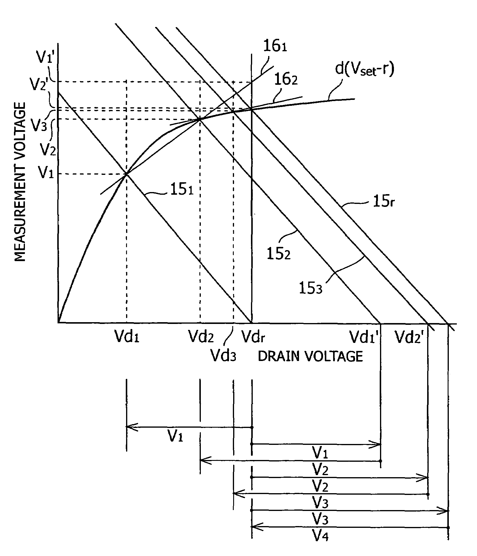
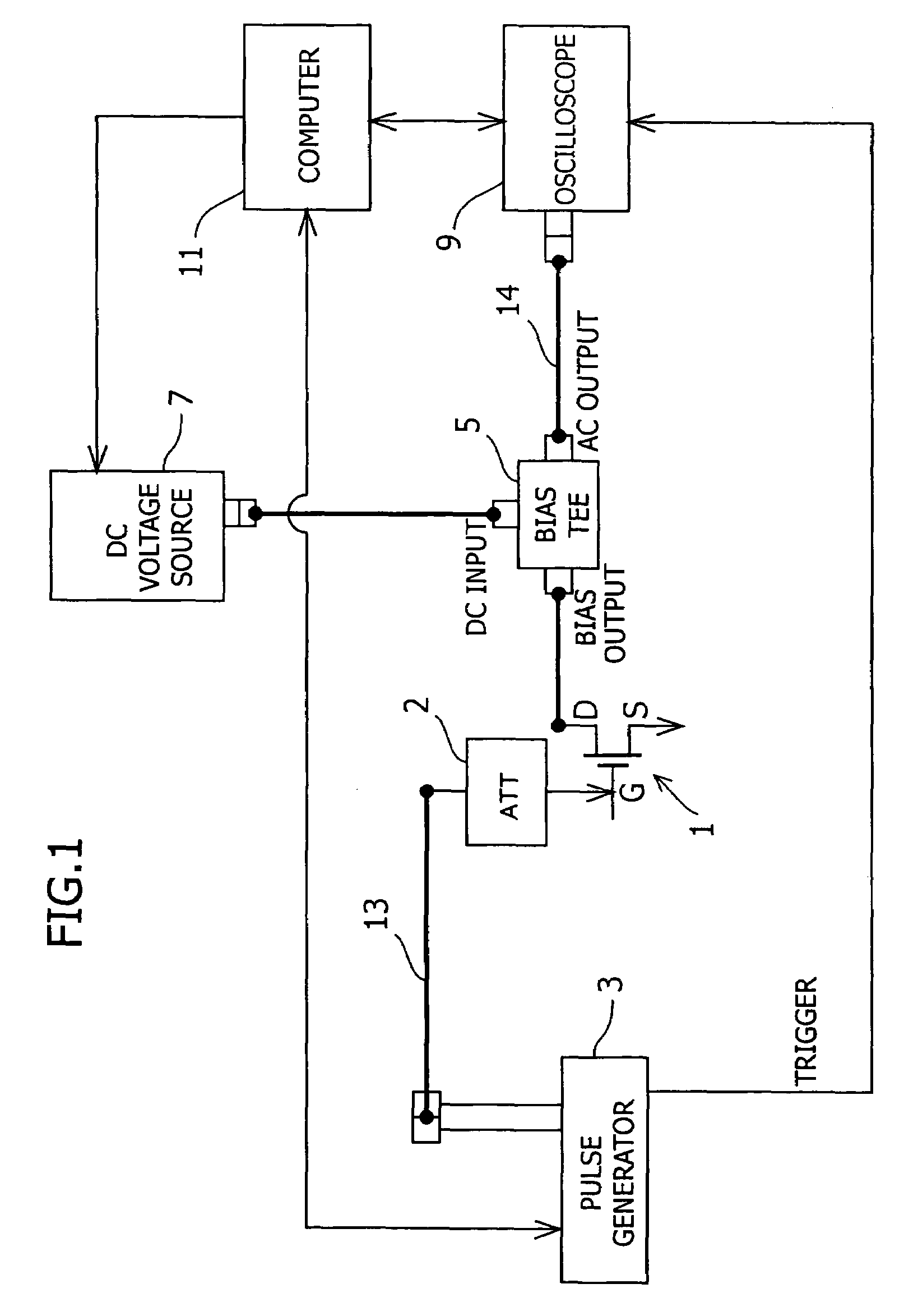
[0025]Referring to FIG. 1, a DUT (device under test) 1 is a MOSFET which may be manufactured by SOI (silicon-on-insulator) technology or strained-silicon fabrication technology.

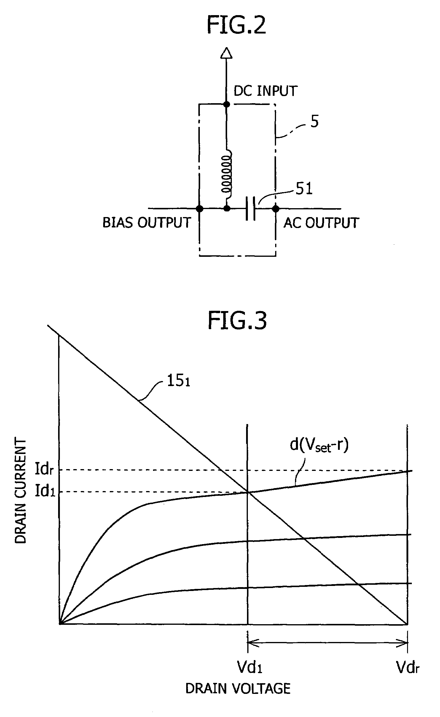
[0026]A pulse generator 3 is connected to the gate (G) of the DUT 1 via an attenuator 2, and a DC voltage source 7 and an oscilloscope 9 (which may be a digital oscilloscope) are connected to the drain (D) of the DUT 1 via a so-called “bias tee”5.

[0027]The DC voltage source 7 may be implemented with an SMU (source measure unit) having the functions of applying highly accurate DC voltages and measuring currents with high accuracy. Examples include the SMU 4156 manufactured by Agilent Technologies Inc.

[0028]In this embodiment, the output impedance of the pulse generator 3 and the input impedance of the oscilloscope 9 are set to 50 Ω. The pulse generator 3 supplies a trigger signal (i.e., a synchroniz...


PUM


Abstract

In an FET-characteristic measuring method, a predetermined bias voltage output from an output terminal of a bias tee is applied to the drain of an FET, and a pulse output from a pulse generator is applied to the gate thereof to thereby cause drain current to be generated. The drain current is converted by a load impedance, connected to an AC output terminal of the bias tee, into a voltage pulse, and is measured based on the voltage pulse. The method includes increasing the bias voltage by an amount corresponding to a voltage drop caused by the load impedance and repeating measurement of a value of the voltage pulse a predetermined number of times, and applying extrapolation to the last two values of the voltage-pulse values obtained by the predetermined number of repeated measurements to determine a drain voltage to be applied to the FET.

Description

BACKGROUND OF THE INVENTION AND RELATED ART STATEMENT[0001]1. Field of the Invention[0002]The present invention relates to methods for inputting pulse signals to the gates of FETs (field-effect transistors) and measuring the IV (current-voltage) characteristics of the FETs. More specifically, the present invention relates to a method preferably used for measuring the IV characteristics of advanced FETs, such as MOSFETs (metal oxide semiconductor field-effect transistors) manufactured by SOI (silicon-on-insulator) technology or strained-silicon fabrication technology.[0003]2. Description of the Related Art[0004]The IV characteristic of an FET is determined by measuring a drain current flowing when a predetermined DC (direct current) voltage is applied to the gate of the FET, while a predetermined bias voltage is applied to the drain of the FET.[0005]However, when the IV characteristics of an advanced FET, such as a MOSFET, manufactured by SOI technology or strained-silicon fabricatio...

Claims


Application Information

Patent Timeline
Patent Type & Authority Patents(United States)
IPC IPC(8): G01R31/26
CPCG01R31/2601G01R31/2621
Inventor SAITO, NOBORU
Owner AGILENT TECH INC
Why Eureka
Try Eureka