System for measuring FET characteristics
- Summary
- Abstract
- Description
- Claims
- Application Information
AI Technical Summary
Benefits of technology
Problems solved by technology
Method used
Image
Examples
Embodiment Construction
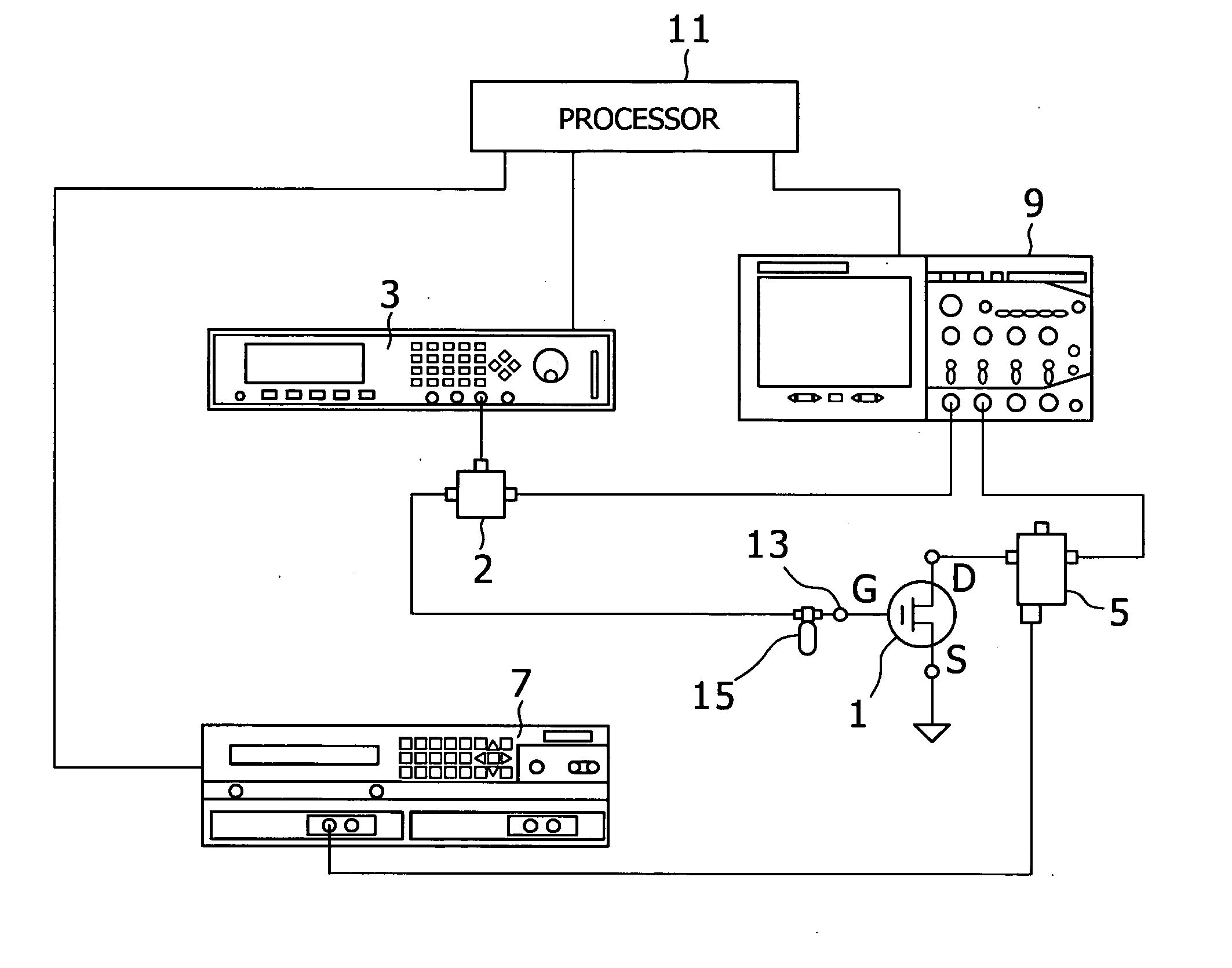
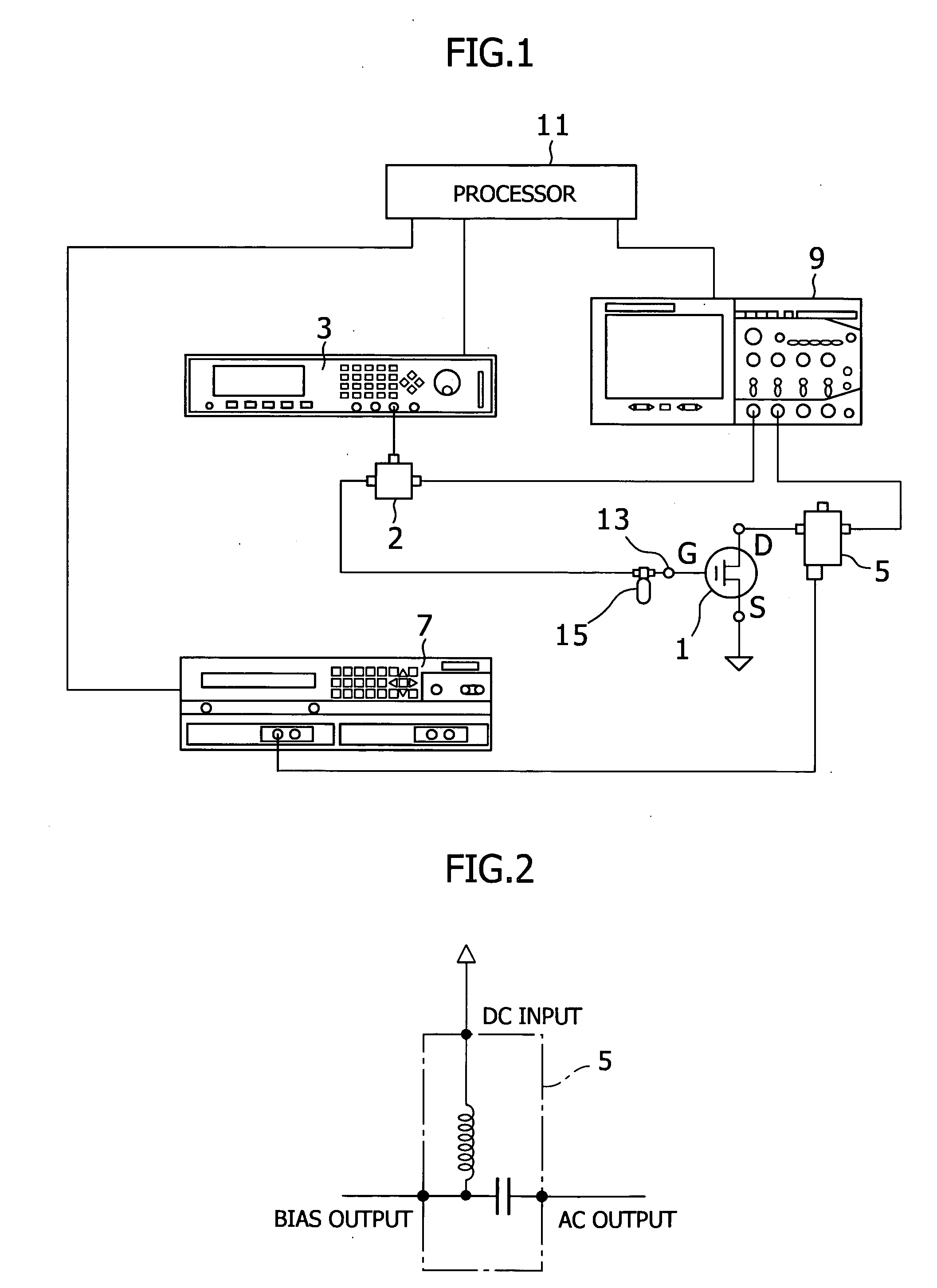
[0018]FIG. 1 is a block diagram illustrating the configuration of an FET-characteristic measuring system according to the present invention. This FET-characteristic measuring system applies a short-duration pulse (e.g., 100 ns or less) to an FET 1 to measure the IV (current-voltage) characteristic thereof
[0019] The FET 1 shown in FIG. 1 is a MOSFET manufactured by SOI (silicon on insulator) technology or strained-silicon fabrication technology.
[0020] The gate of the FET 1 is connected to the pulse generator 3 via a divider 2, and the drain of the FET 1 is connected to a current / voltage source 7 and a terminal (channel 2 in the example shown in FIG. 1) of an oscilloscope 9 (which may be a digital oscilloscope) via a so-called bias tee 5.
[0021] The DC voltage source 7 may be implemented with, for example, an SMU (source measure unit) capable of applying a high-accuracy DC voltage and measuring a current.
[0022] An example of the SMU is Agilent 4156 manufactured by Agilent Technolog...
PUM
 Abstract
Description
Claims
Application Information


