

Holding and positioning apparatus for an optical element
a technology of holding and positioning apparatus, applied in the direction of microlithography exposure apparatus, mountings, instruments, etc., can solve the problems of blurred structures to be imaged in the projection objective of semiconductor lithography during the exposure process, undesired contrast loss, and reduced objective resolution, etc., to achieve the effect of being permissibl
- Summary
- Abstract
- Description
- Claims
- Application Information
AI Technical Summary
Benefits of technology
Problems solved by technology
Method used
Image

Examples
Embodiment Construction
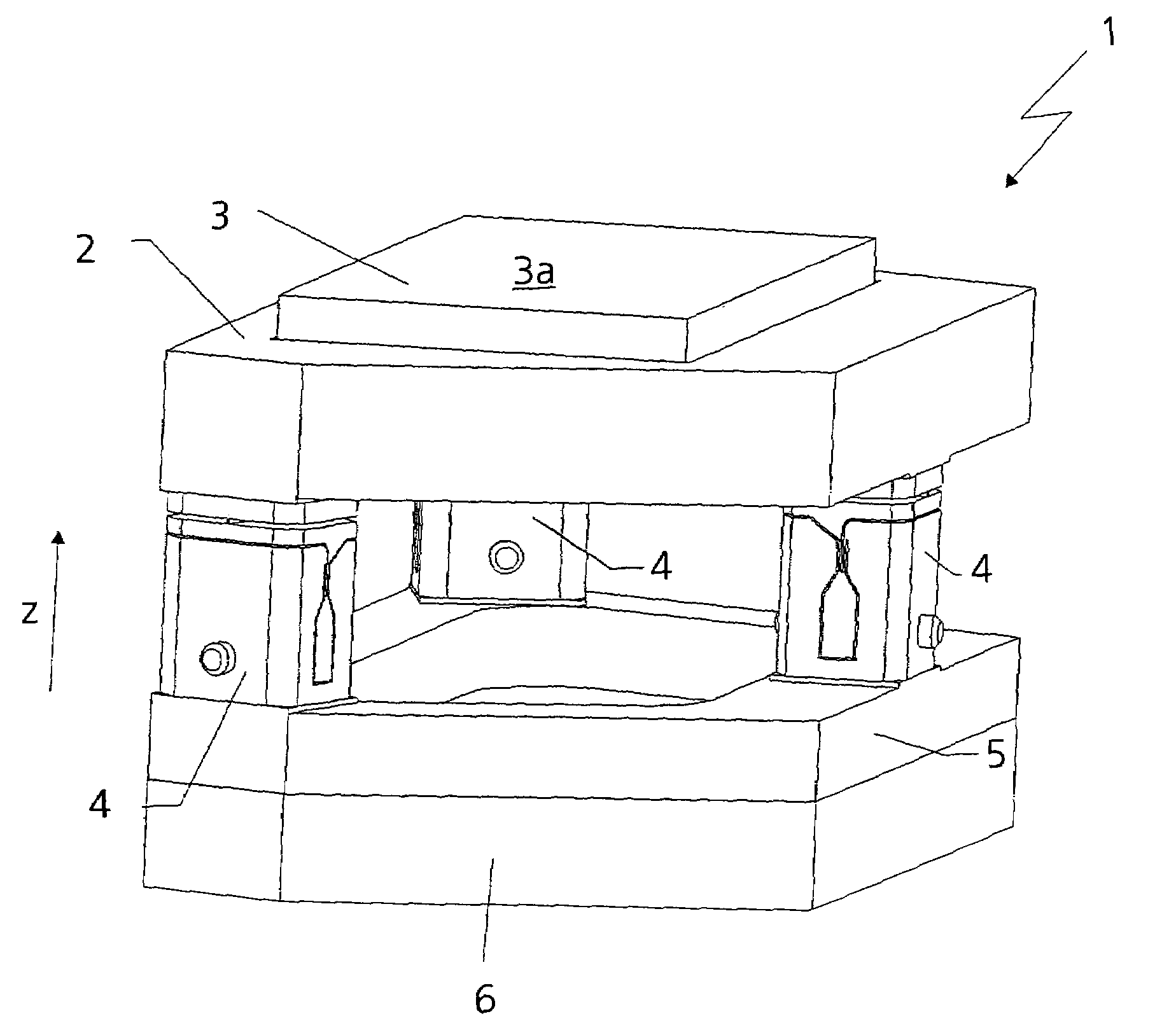
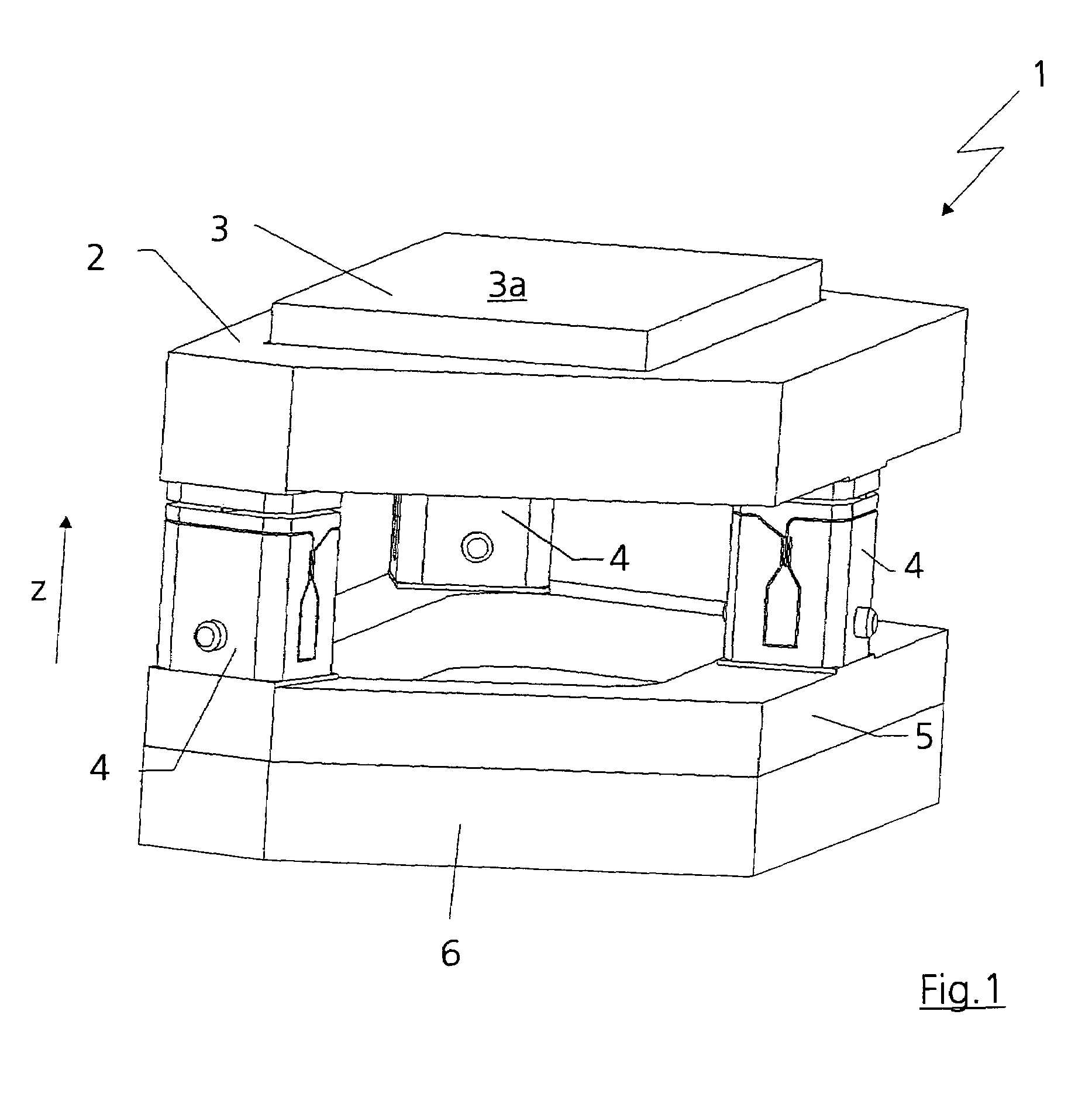
[0028]FIG. 1 shows a holding and positioning apparatus 1 for a projection objective for semiconductor lithography, an optical element 3 being mounted in a mounting ring 2. The optical element 3 is formed as a mirror, preferably as a deflection mirror. The mounting ring 2 is carried and supported by three manipulator units 4, which are firmly connected to a base body 5. The base body 5 is connected in the usual way to a housing (objective housing) or a structure 6. The three manipulator units 4 can be adjusted vertically independently of one another along an optical axis (in the z direction), by which means the mounting ring 2 together with the mirror 3 can be raised at right angles to a mirror plane 3a or tilted about at least one arbitrary axis in the mirror plane 3a.
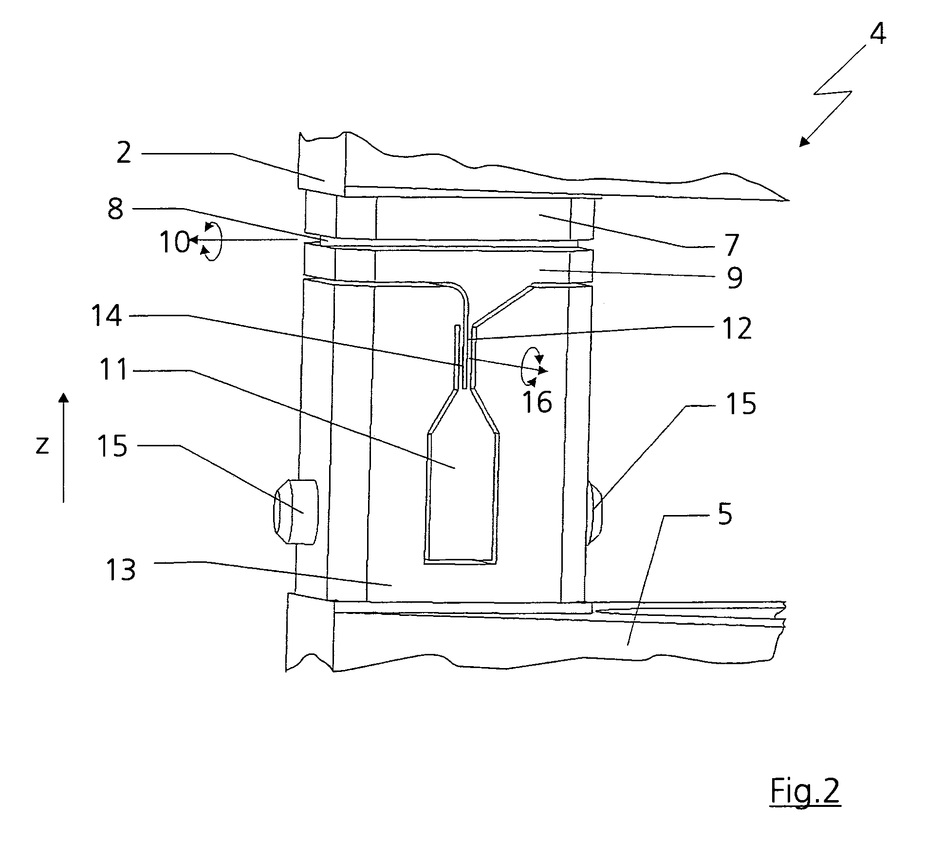
[0029]In FIG. 2, the manipulator unit 4 is illustrated in principle. The manipulator unit 4 has a manipulator head 7 which is connected to the mounting ring 2. The manipulator head 7 is connected to a movable manipula...
PUM
| Property | Measurement | Unit |
|---|---|---|
| angle | aaaaa | aaaaa |
| angle | aaaaa | aaaaa |
| angle | aaaaa | aaaaa |
Abstract
Description
Claims
Application Information