Semiconductor memory device and test pattern data generating method using the same

a memory device and memory technology, applied in the field of semiconductor memory devices, can solve the problems of short supply of mrs codes that could be put to other uses, and achieve the effect of reducing the number of mrs codes

Active Publication Date: 2007-08-14
SAMSUNG ELECTRONICS CO LTD
View PDF7 Cites 6 Cited by
  • Summary
  • Abstract
  • Description
  • Claims
  • Application Information

AI Technical Summary

Benefits of technology

[0008]Embodiments of the invention provide a semiconductor memory device and a test pattern generating method using the same that can reduce the number of MRS codes used to set a test pattern data during a parallel bit test.

Problems solved by technology

Therefore, the conventional semiconductor memory device requires large numbers of MRS codes for a parallel bit test and thus MRS codes that could be put to other uses are in short supply.

Method used


Image

  • Semiconductor memory device and test pattern data generating method using the same
  • Semiconductor memory device and test pattern data generating method using the same
  • Semiconductor memory device and test pattern data generating method using the same

Examples


Embodiment Construction

[0015]The invention will now be described more fully hereinafter with reference to the accompanying drawings, in which preferred embodiments of the invention are shown. This invention may, however, be embodied in different forms and should not be construed as limited to the embodiments set forth herein. Rather, these embodiments are provided so that this disclosure will be thorough and complete, and will fully convey the scope of the invention to those skilled in the art. In the drawings, the thickness of layers and regions are exaggerated for clarity. Like numbers refer to like elements throughout the specification.

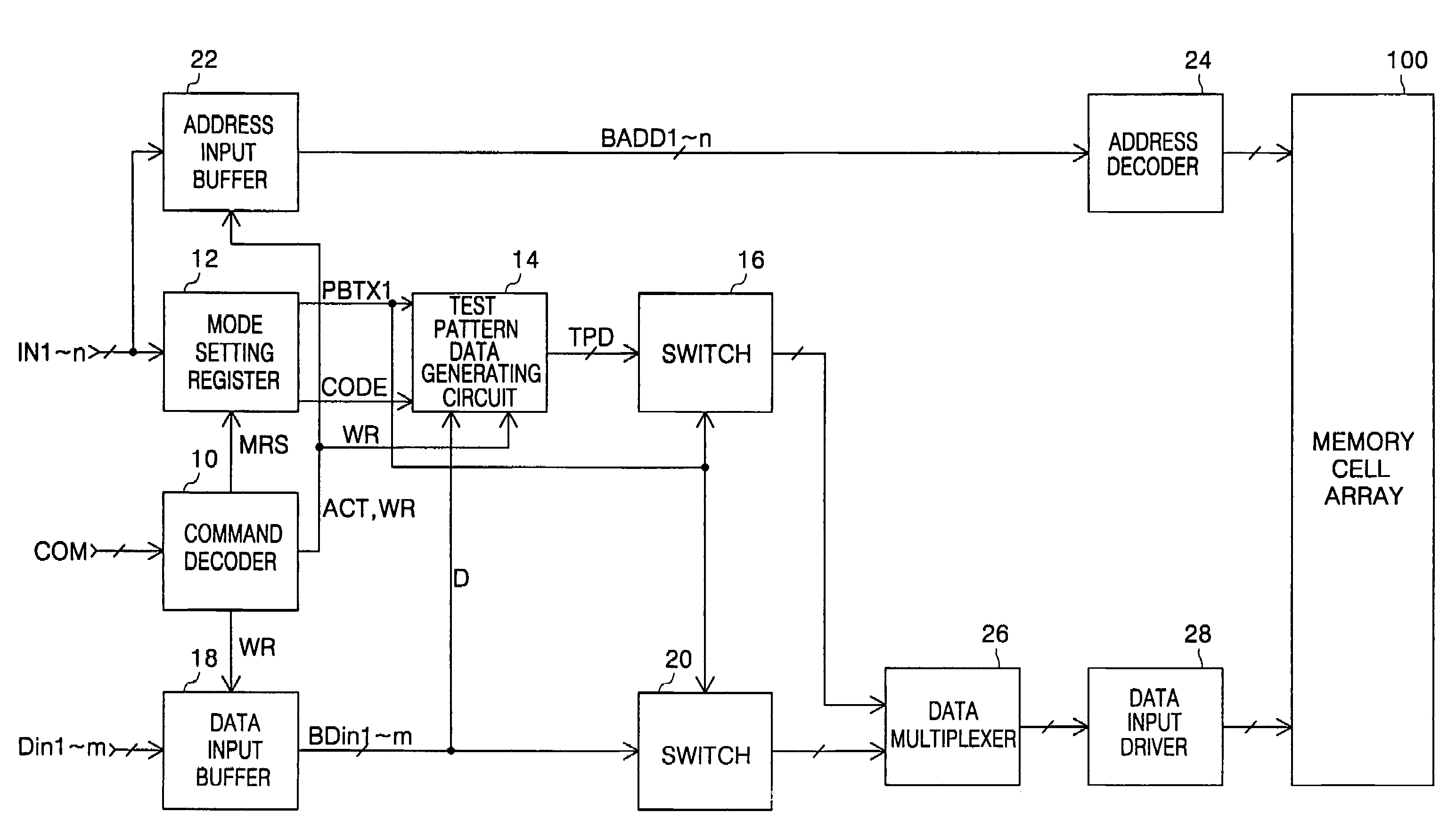
[0016]FIG. 1 a block diagram illustrating a semiconductor memory device according to some embodiments of the invention. The semiconductor memory device of FIG. 1 includes a command decoder 10, a mode setting register 12, a test pattern data generating circuit 14, switches 16 and 20, a data input buffer 18, an address input buffer 22, an address decoder 24, a data multipl...


PUM


Abstract

A semiconductor memory device includes a mode setting register for generating a parallel bit test signal and a code according to an externally applied mode setting register code in response to a mode setting command; a data input circuit for receiving and outputting at least one bit of externally applied data in response to a write command; and a test pattern data generating circuit for receiving the parallel bit test signal and a predetermined bit from the code to generate a test pattern data in response to the at least one bit of externally applied data received from the data input circuit.

Description

CROSS-REFERENCE TO RELATED APPLICATION[0001]This application claims priority from Korean Patent Application No. 2003-80726, filed Nov. 14, 2003, the disclosure of which is hereby incorporated herein by reference in its entirety for all purposes.BACKGROUND OF THE INVENTION[0002]1. Field of the Invention[0003]This disclosure relates to a semiconductor memory device and, more particularly, to a semiconductor memory device that can reduce the number of mode setting register codes used to set a test pattern data during a parallel bit test and a method of generating a test pattern data using the same.[0004]2. Description of the Related Art[0005]A conventional semiconductor memory device has to set and input different mode register setting codes (hereinafter, referred to as simply “MRS codes”) with respect to respective test patterns in order to write a test pattern during a parallel bit test. If the conventional semiconductor memory device is able to internally generate a total of 16 uniq...

Claims


Application Information

Patent Timeline
Patent Type & Authority Patents(United States)
IPC IPC(8): G01R31/28G11C29/00G06F11/00G11C29/14G11C29/34G11C29/36
CPCG11C29/36G11C2029/3602G11C29/00
Inventor CHAE, MOO-SUNGCHOI, HYE-IN
Owner SAMSUNG ELECTRONICS CO LTD
Why Eureka
Try Eureka