Jitter applying circuit and test apparatus

a jitter and test circuit technology, applied in the field of jitter applying circuit and test apparatus, can solve the problems of increasing the circuit scale, difficult to apply large-amplitude and high-resolution jitter by the conventional jitter applying device, and affecting the accuracy of clock signals, etc., to achieve the effect of ensuring the application of clock signals

Active Publication Date: 2007-10-23
ADVANTEST CORP
View PDF9 Cites 18 Cited by
  • Summary
  • Abstract
  • Description
  • Claims
  • Application Information

AI Technical Summary

Problems solved by technology

However, it has been difficult to apply large-amplitude and high-resolution jitter by the conventional jitter applying devices.
When the shift resisters are used for the variable delay circuit for instance, a very large number of registers must be used to apply large-amplitude and high-resolution jitter, increasing the circuit scale enormously.
The same problem also occurs even when another configuration is used for the variable delay circuit.
Still more, in case of generating an oscillating signal containing a jitter component by superimposing the jitter component to control voltage of a voltage controlled oscillator of a PLL circuit, high-frequency jitter cannot be applied because the control voltage is supplied to the voltage controlled oscillator via a low-pass filter.

Method used


Image

  • Jitter applying circuit and test apparatus
  • Jitter applying circuit and test apparatus
  • Jitter applying circuit and test apparatus

Examples


Embodiment Construction

[0022]The invention will now be described based on preferred embodiments, which do not intend to limit the scope of the invention, but exemplify the invention. All of the features and the combinations thereof described in the embodiments are not necessarily essential to the invention.

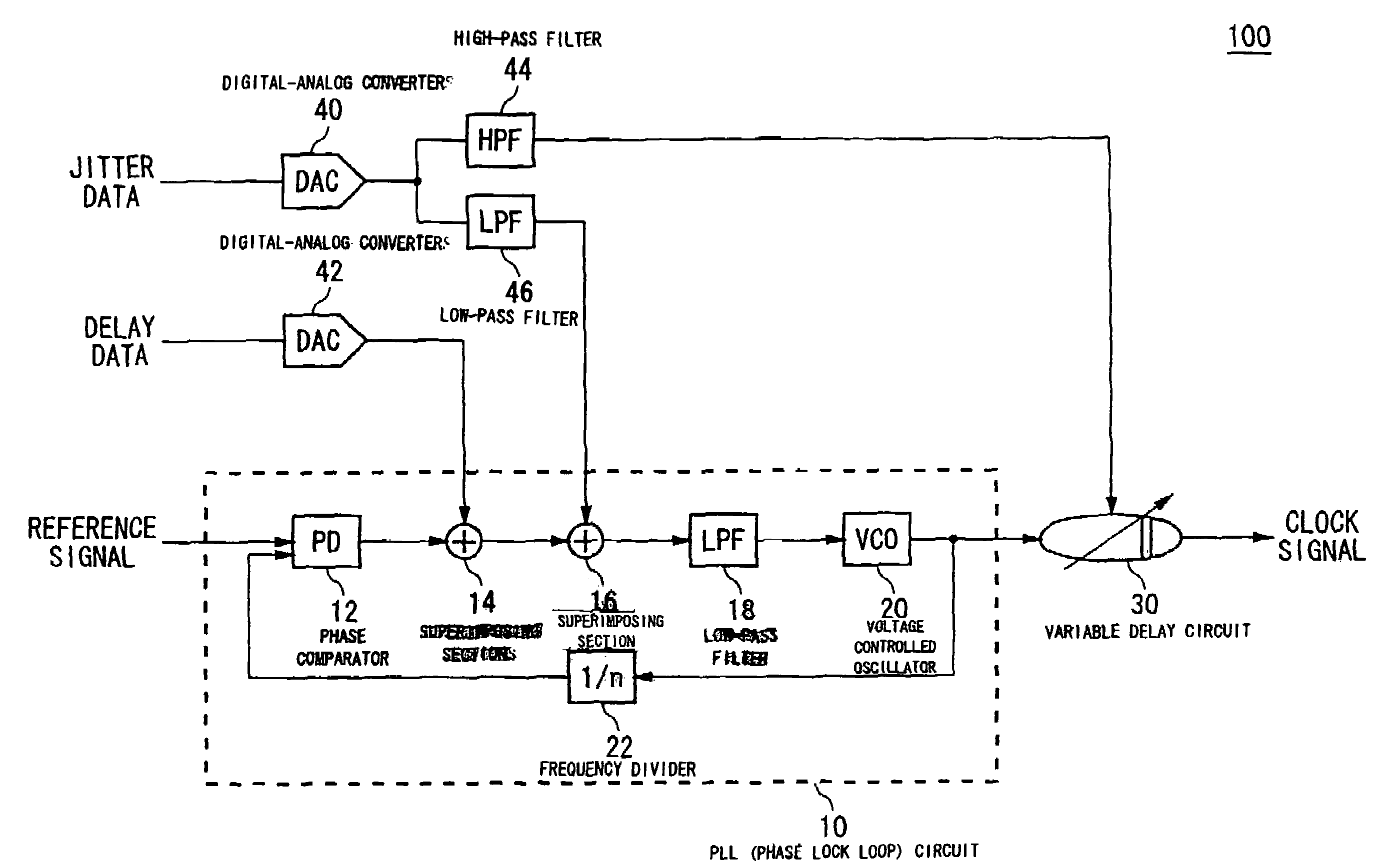
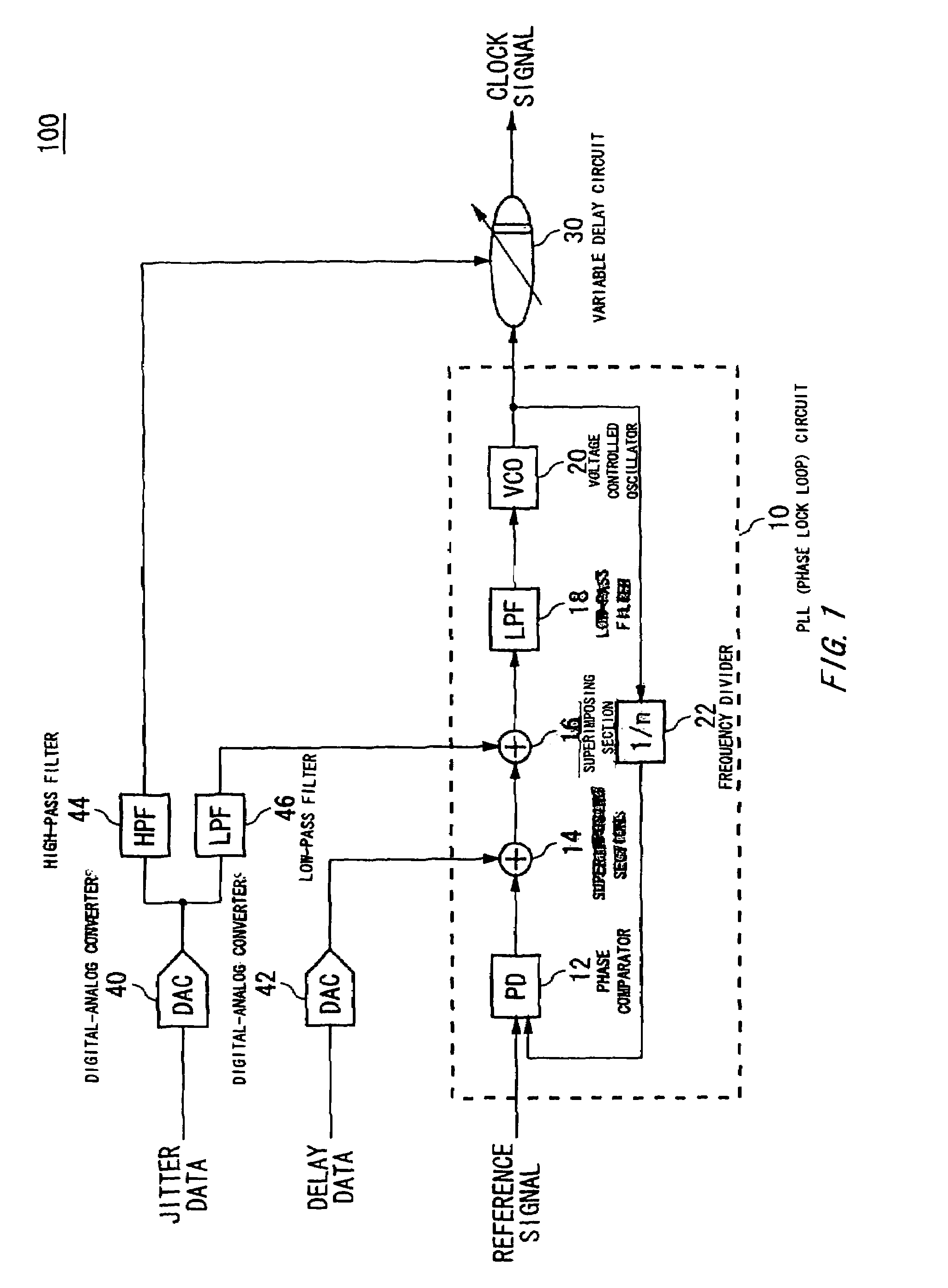
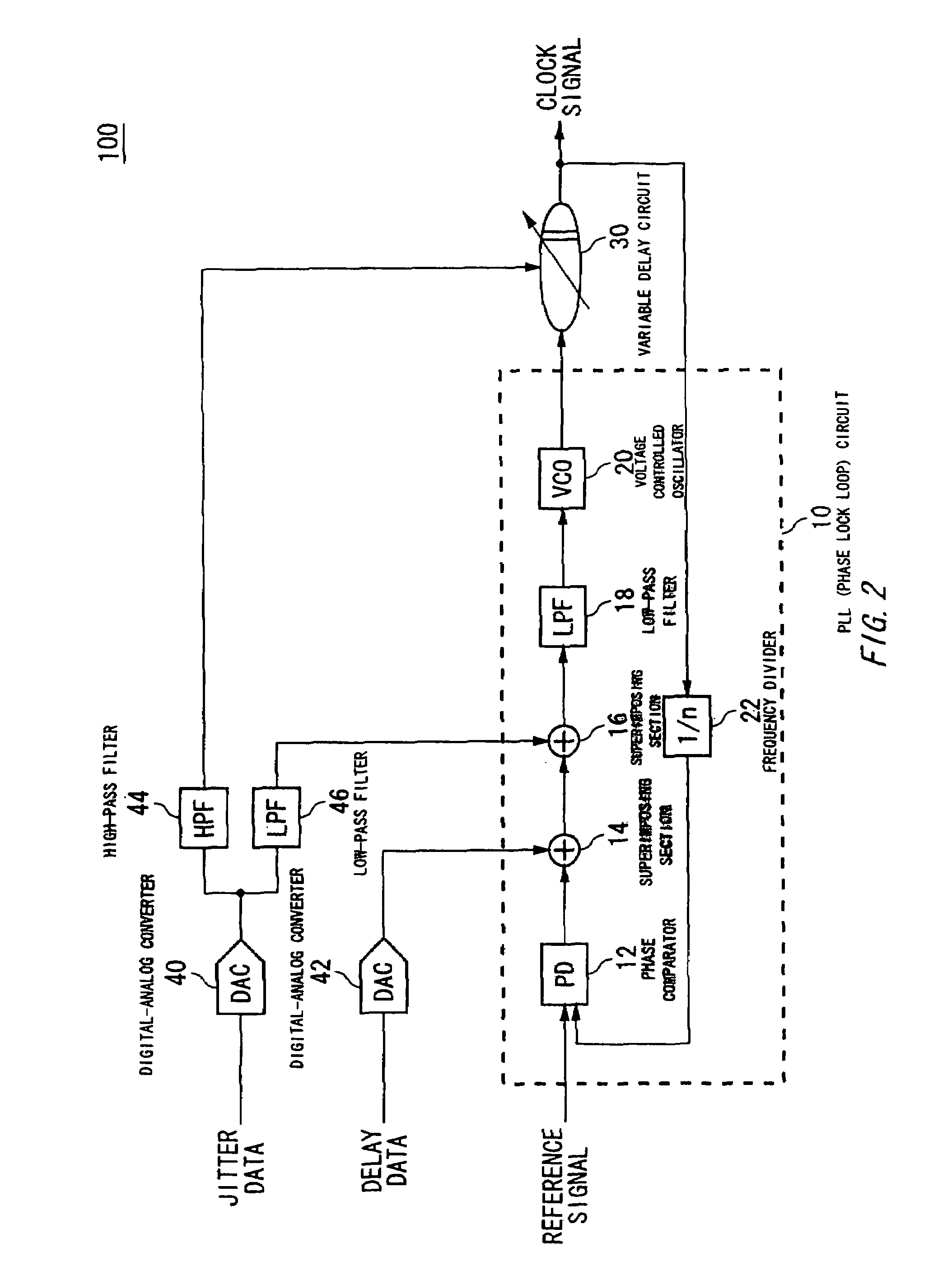
[0023]FIG. 1 is a diagram showing one exemplary configuration of a jitter application circuit 100 according to a mode for carrying out the invention. The jitter application circuit 100 generates a clock signal containing a phase jitter component corresponding to given jitter data and outputs the clock signal containing the phase jitter component with desirable phase. The jitter application circuit 100 has a PLL (Phase Lock Loop) circuit 10, digital-analog converters 40 and 42 (hereinafter abbreviated as DACs 40 and 42), a high-pass filter 44, a low-pass filter 46 and a variable delay circuit 30. A delay for controlling the phase jitter component to be applied to the clock signal and for controlling the ...


PUM

PropertyMeasurementUnit
phase jitteraaaaaaaaaa
oscillation frequencyaaaaaaaaaa
frequencyaaaaaaaaaa

Abstract

There is provided a jitter application circuit for generating a clock signal containing a phase jitter component corresponding to given jitter data, having a PLL circuit for generating an oscillating signal corresponding to a given reference signal, a variable delay circuit for outputting said clock signal in which said oscillating signal is delayed, a low-frequency application section for applying low-frequency component of said phase jitter component to said oscillating signal by controlling oscillation frequency of said PLL circuit based on the low-frequency component of said jitter data and a high-frequency application section for applying high-frequency component of said phase jitter component to said clock signal by controlling a delay in said variable delay circuit based on the high-frequency component of said jitter data.

Description

[0001]The present application is a continuation application of PCT / JP2005 / 011589 filed on Jun. 24, 2005 which claims the priority from Japanese Patent Application No. 2004-214888 filed on Jul. 22, 2004 and whose content is incorporated in the present application by reference as part of description thereof.BACKGROUND OF THE INVENTION[0002]1. Field of the Invention[0003]The present invention relates to a jitter application circuit for generating a clock signal containing a phase jitter component corresponding to given jitter data and a test apparatus for testing jitter resistance of electronic devices.[0004]2. Related Art[0005]Conventionally, as a circuit for applying jitter into a clock signal, there has been known a jitter applying device that controls a delay of a variable delay circuit for delaying and outputting such clock signal corresponding to jitter to be given. The applicant of the present application has proposed a jitter applying device that controls the delay of the varia...

Claims


Application Information

Patent Timeline
Patent Type & Authority Patents(United States)
IPC IPC(8): G11B20/20G06F11/00H03L7/06
CPCH03L7/081G01R31/31727H03K5/156G01R31/30G01R31/3183H03L7/18
Inventor MIYAJI, YUICHI
Owner ADVANTEST CORP
Why Eureka
Try Eureka