Molecular memory devices and methods

a molecular memory and molecular memory technology, applied in the field of memory devices, can solve the problems of capacitors being inherently “leaky” devices, affecting at least some of these important parameters, and the size of conventional semiconductor memory cells continues to be reduced

Inactive Publication Date: 2007-12-11
ZETTACORE
View PDF45 Cites 25 Cited by
  • Summary
  • Abstract
  • Description
  • Claims
  • Application Information

AI Technical Summary

Problems solved by technology

Unfortunately, conventional silicon-based memory, such as DRAM memory, has reached a point where continued reduction in the size of conventional semiconductor memory cells is expected to adversely affect at least some of these important parameters.
Moreover, capacitors are inherently “leaky” devices in that some of the charge stored in a capacitor dissipates or leaks over time.
Memory devices based on smaller capacitors are more sensitive to leakage problems because they simply have less charge that can be lost before the stored data becomes irretrievable.
Moreover, a greater percentage of the total power consumption of the memory device is then used to refresh the memory.
Even when the device is in a dormant or inactive state, traditional DRAM requires continuous refreshing and therefore continuous power consumption.
Boosting capacitance often involves increasing the surface area of the capacitor's charge holding material, which is very difficult to do when the overall size of the capacitor is shrinking.
While designers have had some success at controlling surface area by forming the charge holding material into three-dimensional trench and stacked capacitor designs, it is unlikely that these techniques can be relied for continued progress rendering larger capacitances in smaller devices.
The solid state electronic behaviors upon which device performance is predicated begin to break down as the dimensions of various device features become smaller such that a capacitor can no longer store sufficient charge for sufficient time to be useful in a memory device.
Another problem facing memory designers trying to increase information density (e.g., the amount of information that can be stored in a given area of the memory chip).

Method used


Image

  • Molecular memory devices and methods
  • Molecular memory devices and methods
  • Molecular memory devices and methods

Examples


Embodiment Construction

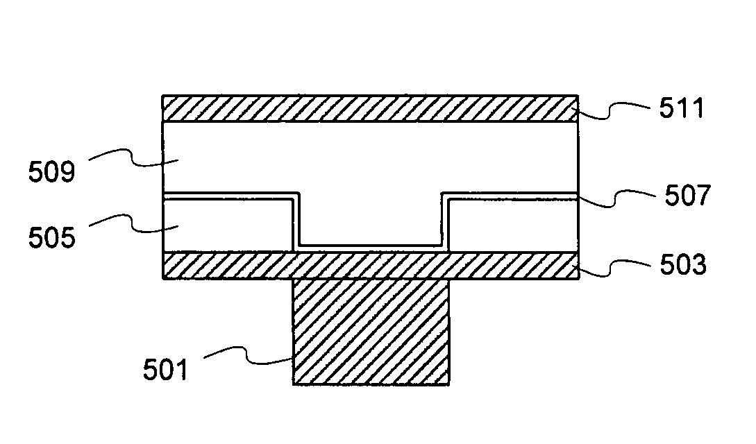
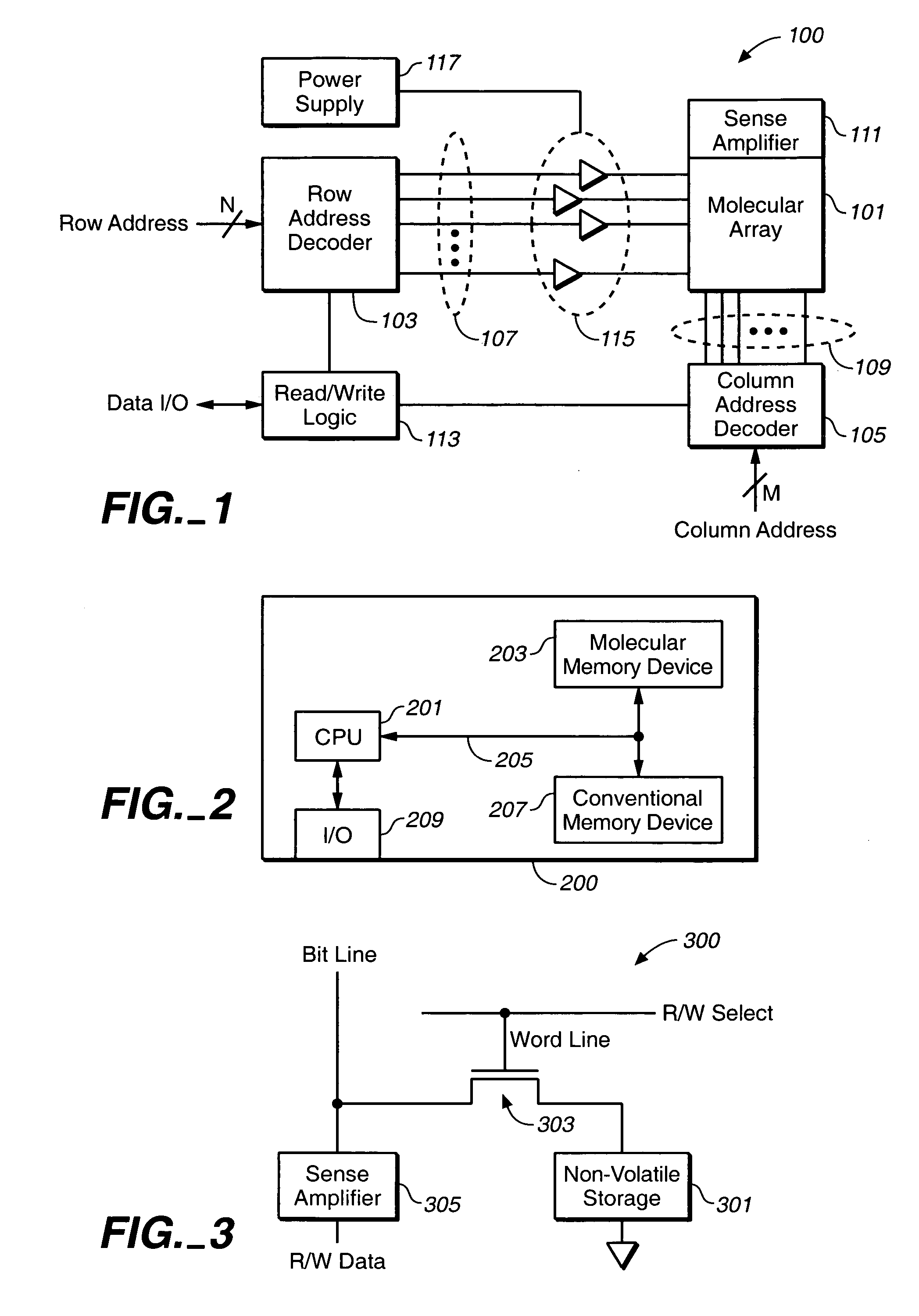
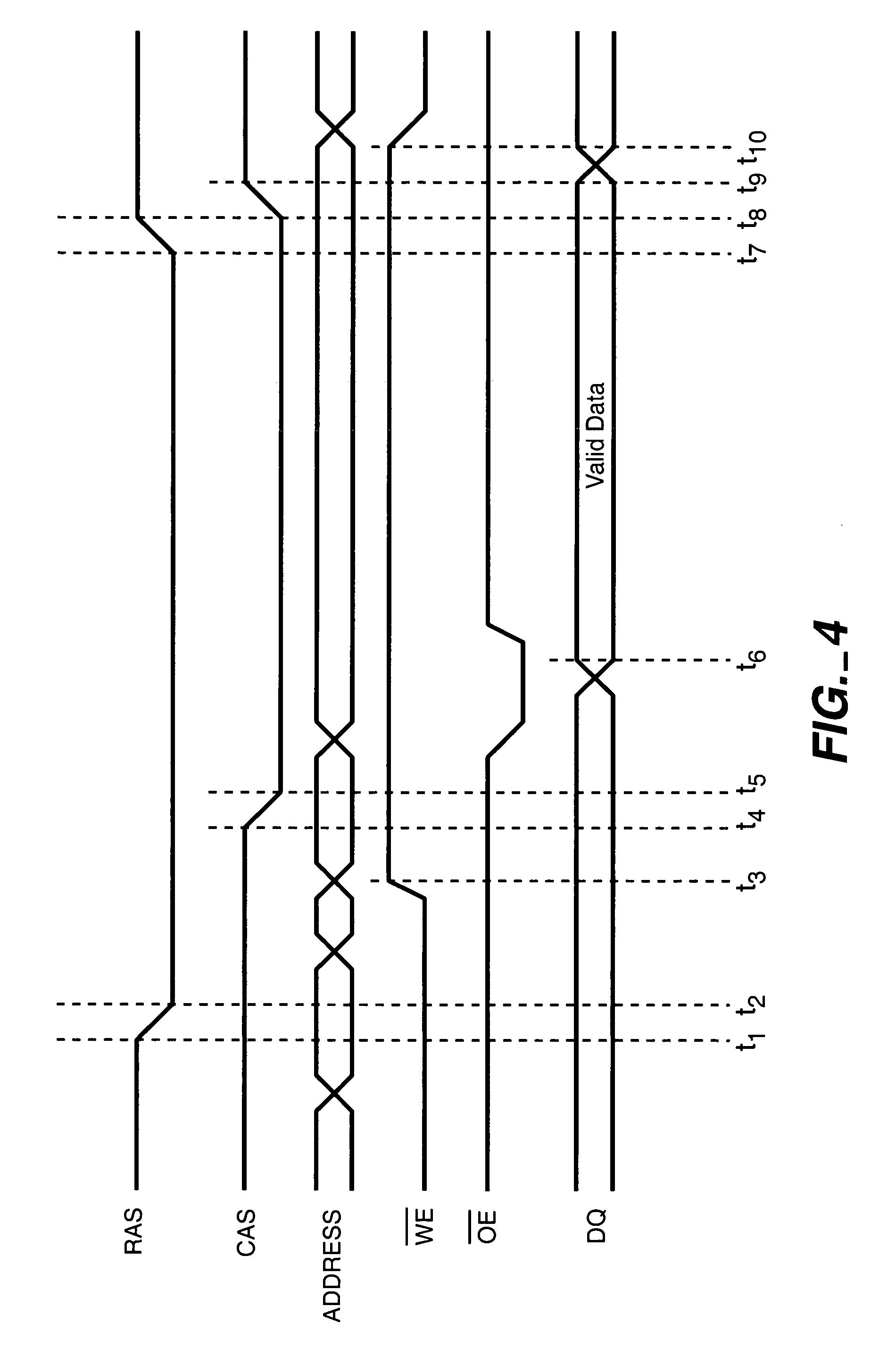
[0039]The present invention contemplates a number of device and system architectures that enable the use of molecular memory elements (sometimes referred to herein and in related applications as “storage molecules” or “memory molecules”) to be integrated with and benefit from the technology developed for conventional microelectronics. At one level the present invention involves molecular memory elements that integrate storage molecules with switching logic that enables reading and writing to the storage molecules. At another extreme, the represent invention contemplates highly integrated circuits having logic devices, including data processing circuitry, integrated monolithically with molecular memory arrays to provide new and useful functions that leverage one or more the unique features of molecular memory such as lower power usage, superior data persistence, higher information density, and the like.

[0040]There are a wide variety of suitable storage molecules for use in the presen...


PUM


Abstract

A molecular memory element comprising a switching device; at least a first bit line and a first word line coupled to said switching device; and an array of storage locations, each coupled to a bit line and a word line, said elements comprising a first electrode with storage molecules comprising redox active molecules, and said array comprising a second electrode.

Description

[0001]This application is a continuation application of U.S. application Ser. No. 11 / 046,518, filed on Jan. 28, 2005 now abandoned, which is a Continuation-in-Part of U.S. application Ser. No. 10 / 766,304, filed on Jan. 28, 2004, now abandoned all which are hereby incorporated by reference in their entirety.FIELD OF THE INVENTION[0002]This invention relates to memory devices, such as static, permanent and dynamic random access memory. In particular, this invention relates to molecular memory cells, molecular memory arrays, and electronic devices including molecular memory, particularly logic devices.BACKGROUND OF THE INVENTION[0003]Advances in semiconductor processing and device design have resulted in computing devices being incorporated with a seemingly endless variety of tools and machines ranging from conventional programmable computers to communication equipment and entertainment devices. Irrespective of its end purpose, a computing device is generally made up of three main comp...

Claims


Application Information

Patent Timeline
Patent Type & Authority Patents(United States)
IPC IPC(8): G11C11/00
CPCB82Y10/00G11C11/5664G11C13/0014G11C13/0016G11C13/0009G11C2213/79
Inventor KUHR, WERNER G.GALLO, ANTONIO R.
Owner ZETTACORE
Why Eureka
Try Eureka