Process for making and programming and operating a dual-bit multi-level ballistic flash memory

a ballistic flash memory and multi-level technology, applied in the field of high-density flash memory arrays, can solve the problems of high program voltage of about 12v, interference with bit line signals, and inability to detect multi-level thresholds,

Inactive Publication Date: 2000-10-17
HALO LSI DESIGN & DEVICE TECH
View PDF8 Cites 263 Cited by
  • Summary
  • Abstract
  • Description
  • Claims
  • Application Information

AI Technical Summary

Problems solved by technology

In this approach, if the selected cell has a low threshold and the bit line drops below VDD-Vt, then the adjacent cell which shares the same bit line may also start to conduct, depending on its threshold state, and interfere with the bit line signal.
This stipulation renders sensing of multi-level thresholds difficult, if not impossible.
Some of the disadvantages of the DSG cell are high program voltages of about 12V and also high voltages during read.
Erase of a single cell is not possible.
Short program pulses and frequent program verify operations will result in tight Vt distributions; however the overall program time is long because time is wasted during verify and switching between the program and verify modes.

Method used


Image

  • Process for making and programming and operating a dual-bit multi-level ballistic flash memory
  • Process for making and programming and operating a dual-bit multi-level ballistic flash memory
  • Process for making and programming and operating a dual-bit multi-level ballistic flash memory

Examples


Embodiment Construction

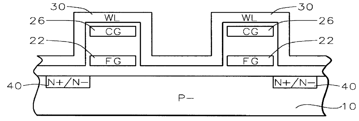
Read operation for a two bit multi-level storage in each of the floating gates will be described, based on simulations for a 0.25 .mu. process. FIG. 7A illustrates the memory cell and voltage conditions for a read of floating gate 313. The threshold voltages for the four levels of storage are 0.8V, 1.2V, 1.6V, and 2.0V for the "11", "10", "01", and "00" states, respectively. This is shown in FIG. 7B. The threshold voltage for the word select gate is 0.5V. The capacitance coupling ratios between the control gate to floating gate, word gate to floating gate, and drain to floating gate are 0.55, 0.30 and 0.15, respectively. During read, the source voltage is fixed to 1.2V. The control gate associated with the unselected floating gate is set to 5V, and the control gate associated with the selected floating gate is set to 2.5V. All other control gates are set to zero, and the bit junction is precharged to zero.

When the word line is raised from 0V to 2.5V, based on the capacitance couplin...


PUM


Abstract

An fast program, ultra-high density, dual-bit, multi-level flash memory process, which can be applied to a ballistic step split gate side wall transistor, or to a ballistic planar split gate side wall transistor, which enables program operation by low voltage requirement on the floating gate during program is described. Two side wall floating gates are paired with a single word line select gate, and word lines are arranged to be perpendicular both the bit lines and control gate lines. Two adjacent memory cells on the same word line do not require an isolation region. Also, the isolation region between adjacent memory cells sharing the same bitline is defined by the minimum lithography feature, utilizing a self align fill technique. Adjacent memory cells on the same word line share bitline diffusion as well as a third poly control gate. Control gates allow program and read access to the individual floating gate. In addition to the dual-bit nature of the cell, density can be even further improved by multi-level storage. In one embodiment, the dual multi-level structure is applied to the ballistic step split gate side wall transistor. In a second embodiment, the dual multi-level structure is applied to the ballistic planar split gate side wall transistor. Both types of ballistic transistors provide fast, low voltage programming. The control gates are used to override or suppress the various threshold voltages on associated floating gates, in order to program to and read from individual floating gates. The targets for this non-volatile memory array are to provide the capabilities of high speed, low voltage programming (band width) and high density storage.

Description

1) Field of InventionThe invention relates to methods of forming high-density flash memory arrays and the resulting high density flash memory arrays.2) Description of the Prior ArtIn the NOR-type memory cell, the polysilicon memory select gate is connected to a word line, one floating gate-side diffusion is connected to a source line, and the other diffusion is connected to a bit line. Word lines run parallel to the source lines and perpendicular to the bit lines. Better density may be achieved when the source lines are rotated to run parallel to the bit lines, and then combined into single lines. Such high density flash memory arrays, having interchangeable bit lines / source lines between adjacent cells, have been described in previous works such as U.S. Pat. No. 5,654,917 (IBM) to S, Ogura et al, and U.S. Pat. No. 5,278,439 to Yueh Y. Ma: "Self-aligned dual-bit split gate (DSG) flash EEPROM cell".Referring to FIG. 1, a schematic of the high density array described in U.S. Pat. No. ...

Claims


Application Information

Patent Timeline
Patent Type & Authority Patents(United States)
IPC IPC(8): G11C11/56G11C16/04H01L27/115H01L21/70H01L21/8247
CPCG11C11/5621G11C16/0458G11C16/0475H01L27/11524H01L27/115H01L27/11521G11C2211/5612H10B69/00H10B41/30H10B41/35
Inventor OGURA, SEIKIOGURA, TOMOKO
Owner HALO LSI DESIGN & DEVICE TECH
Why Eureka
Try Eureka